JAJSCH6C June 2016 – June 2021 TPS62135
PRODUCTION DATA
- 1 特長
- 2 アプリケーション
- 3 概要
- 4 Revision History
- 5 Device Comparison Table
- 6 Pin Configuration and Functions
- 7 Specifications
- 8 Parameter Measurement Information
-
9 Detailed Description
- 9.1 Overview
- 9.2 Functional Block Diagram
- 9.3 Feature Description
- 9.4
Device Functional Modes
- 9.4.1 Pulse Width Modulation (PWM) Operation
- 9.4.2 Power Save Mode Operation (PWM/PFM)
- 9.4.3 100% Duty-Cycle Operation
- 9.4.4 HICCUP Current Limit And Short Circuit Protection (TPS62135 only)
- 9.4.5 Current Limit And Short Circuit Protection (TPS621351 only)
- 9.4.6 Soft-Start / Tracking (SS/TR)
- 9.4.7 Output Discharge Function (TPS62135 only)
- 9.4.8 Starting into a Pre-Biased Load (TPS621351 only)
- 10Application and Implementation
- 11Power Supply Recommendations
- 12Layout
- 13Device and Documentation Support
- 14Mechanical, Packaging, and Orderable Information
9.4.4 HICCUP Current Limit And Short Circuit Protection (TPS62135 only)
The TPS62135 is protected against overload and short circuit events. If the inductor current exceeds the current limit I(LIMH), the high side switch is turned off and the low side switch is turned on to ramp down the inductor current. The high side FET turns on again only if the current in the low side FET has decreased below the low side current limit threshold. Once the high side switch current limit is triggered for 512 subsequent switching cycles, the device stops switching. After a typical delay of 800 µs, the device begins a new Soft-Start cycle. This is called HICCUP short circuit protection. TPS62135 repeats this mode until the short circuit condition disappears.
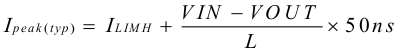
Due to internal propagation delay, the actual current can exceed the static current limit during that time. The dynamic current limit is given as:
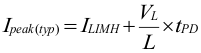
where:
ILIMH is the static current limit as specified in the electrical characteristics
L is the effective inductance at the peak current
VL is the voltage across the inductor (VIN - VOUT) and
tPD is the internal propagation delay of typically 50 ns.
The current limit can exceed static values, especially if the input voltage is high and very small inductances are used. The dynamic high side switch peak current can be calculated as follows: