JAJSCH6C June 2016 – June 2021 TPS62135
PRODUCTION DATA
- 1 特長
- 2 アプリケーション
- 3 概要
- 4 Revision History
- 5 Device Comparison Table
- 6 Pin Configuration and Functions
- 7 Specifications
- 8 Parameter Measurement Information
-
9 Detailed Description
- 9.1 Overview
- 9.2 Functional Block Diagram
- 9.3 Feature Description
- 9.4
Device Functional Modes
- 9.4.1 Pulse Width Modulation (PWM) Operation
- 9.4.2 Power Save Mode Operation (PWM/PFM)
- 9.4.3 100% Duty-Cycle Operation
- 9.4.4 HICCUP Current Limit And Short Circuit Protection (TPS62135 only)
- 9.4.5 Current Limit And Short Circuit Protection (TPS621351 only)
- 9.4.6 Soft-Start / Tracking (SS/TR)
- 9.4.7 Output Discharge Function (TPS62135 only)
- 9.4.8 Starting into a Pre-Biased Load (TPS621351 only)
- 10Application and Implementation
- 11Power Supply Recommendations
- 12Layout
- 13Device and Documentation Support
- 14Mechanical, Packaging, and Orderable Information
10.1.3 Inductor Selection
The TPS62135x is designed for a nominal 1-µH inductor. Larger values can be used to achieve a lower inductor current ripple but they may have a negative impact on efficiency and transient response. Smaller values than 1µH will cause a larger inductor current ripple which causes larger negative inductor current in forced PWM mode at low or no output current. Therefore they are not recommended at large voltages across the inductor as it is the case for high input voltages and low output voltages. With low output current in forced PWM mode this causes a larger negative inductor current peak which may exceed the negative current limit. At low or no output current and small inductor values the output voltage can therefore not be regulated any more. More detailed information on further LC combinations can be found in SLVA463.
The inductor selection is affected by several effects like inductor ripple current, output ripple voltage, PWM-to-PFM transition point and efficiency. In addition, the inductor selected has to be rated for appropriate saturation current and DC resistance (DCR). Equation 9 calculates the maximum inductor current.
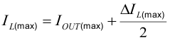
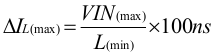
where:
IL(max) is the maximum inductor current
ΔIL is the Peak to Peak Inductor Ripple Current
L(min) is the minimum effective inductor value.
Calculating the maximum inductor current using the actual operating conditions gives the minimum saturation current of the inductor needed. A margin of about 20% is recommended to add. A larger inductor value is also useful to get lower ripple current, but increases the transient response time and size as well. The following inductors have been used with the TPS62135x and are recommended for use:
| TYPE | INDUCTANCE [µH] | CURRENT [A](1) | DIMENSIONS [LxBxH] mm | MANUFACTURER |
|---|---|---|---|---|
| XFL4020-102ME | 1.0 µH, ±20% | 5.4 | 4 x 4 x 2.1 | Coilcraft |
| XAL4020-102ME | 1.0 µH, ±20% | 8.7 | 4 x 4 x 2.1 | Coilcraft |
| XAL4020-152ME | 1.5 µH, ±20% | 7.1 | 4 x 4 x 2.1 | Coilcraft |
| XFL4030-102ME | 1.0 µH, ±20% | 4.1 | 4 x 4 x 3.1 | Coilcraft |
| 1277AS-H-1R0M (DFE322512C) | 1.0 µH, ±20% | 3.1(2) | 3.2 x 2.5 x 1.2 | Murata |
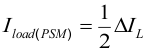
The inductor value also determines the load current at which Power Save Mode is entered: