JAJSCH6C June 2016 – June 2021 TPS62135
PRODUCTION DATA
- 1 特長
- 2 アプリケーション
- 3 概要
- 4 Revision History
- 5 Device Comparison Table
- 6 Pin Configuration and Functions
- 7 Specifications
- 8 Parameter Measurement Information
-
9 Detailed Description
- 9.1 Overview
- 9.2 Functional Block Diagram
- 9.3 Feature Description
- 9.4
Device Functional Modes
- 9.4.1 Pulse Width Modulation (PWM) Operation
- 9.4.2 Power Save Mode Operation (PWM/PFM)
- 9.4.3 100% Duty-Cycle Operation
- 9.4.4 HICCUP Current Limit And Short Circuit Protection (TPS62135 only)
- 9.4.5 Current Limit And Short Circuit Protection (TPS621351 only)
- 9.4.6 Soft-Start / Tracking (SS/TR)
- 9.4.7 Output Discharge Function (TPS62135 only)
- 9.4.8 Starting into a Pre-Biased Load (TPS621351 only)
- 10Application and Implementation
- 11Power Supply Recommendations
- 12Layout
- 13Device and Documentation Support
- 14Mechanical, Packaging, and Orderable Information
10.3.4 Precise Soft-Start Timing
The SS/TR pin of the TPS62135x can be used for tracking as well as for setting the Soft-Start time. The TPS62135x has one GND terminal which is used for the power ground as well as for the analog ground connection. While starting the device with a load current above approximately 1 A, the noise on the GND connection can lead to a Soft-Start time shorter than calculated. There are two external work arounds as given below.
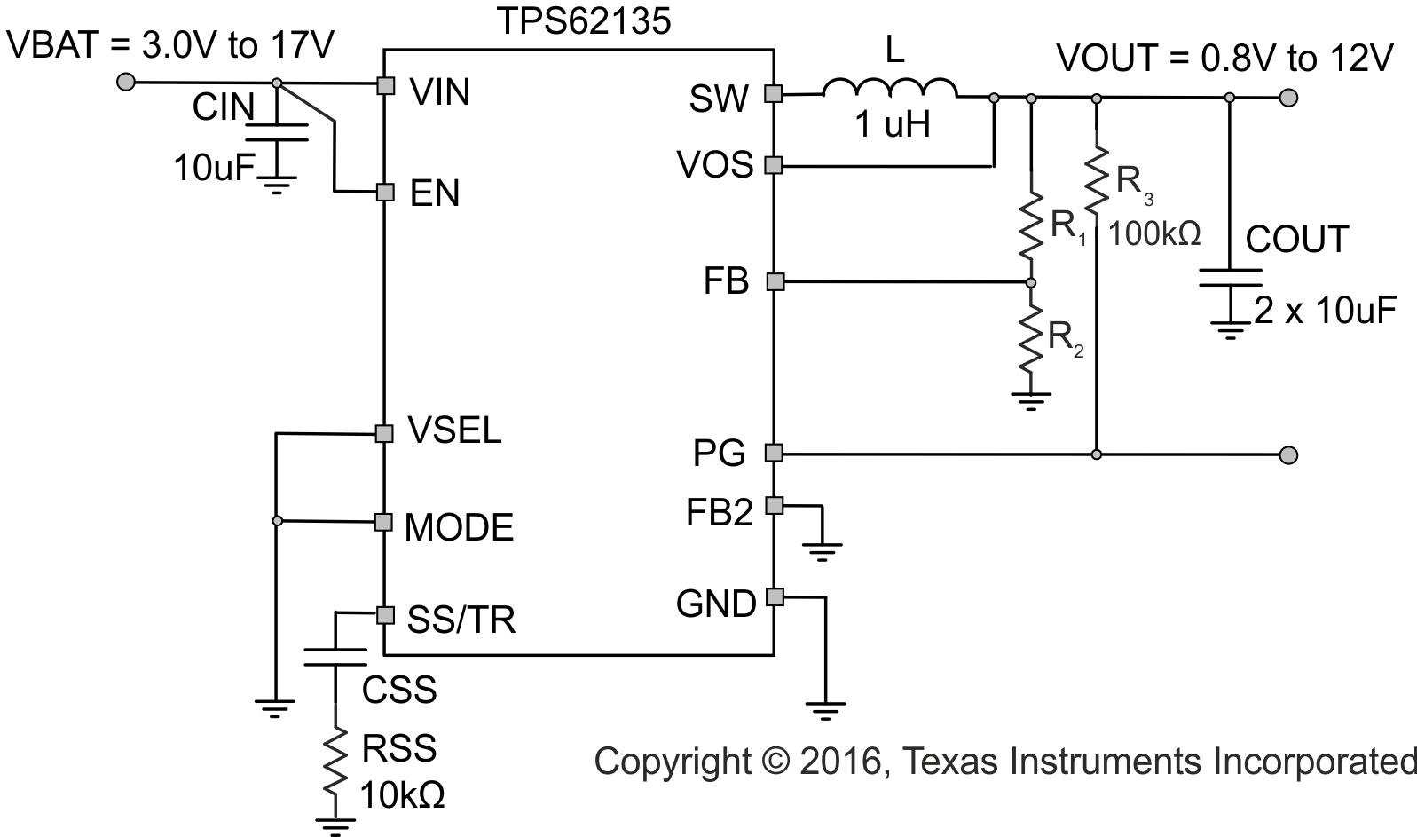
Adding a 10 kΩ resistor filters the noise on the GND connection and keeps the Soft-Start time at the value calculated.
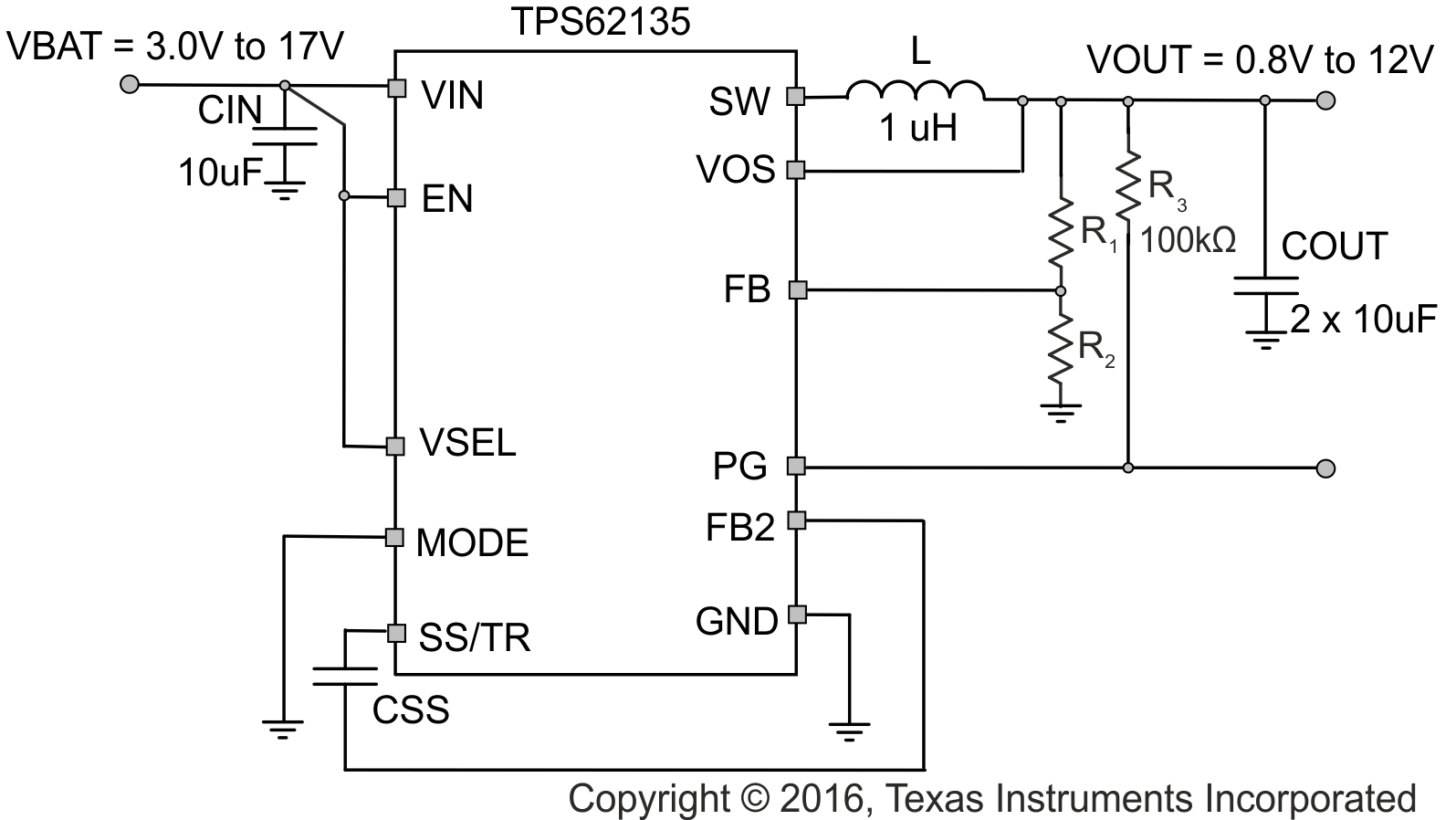
Figure 10-88 does not require an external component. It provides a connection to the internal analog ground by using the FB2 pin and its internal NMOS to that node. The internal NMOS needs to be turned ON by setting VSEL = high.
 Figure 10-87 Adding a Series Resistor to CSS
 Figure 10-88 Connecting CSS to the Internal Analog Ground by using FB2