JAJSH47 March   2019 TPS65653-Q1

PRODUCT PREVIEW Information. Product in design phase of development. Subject to change or discontinuance without notice.  

  1. 特長
    1.     概略回路図
  2. アプリケーション
  3. 概要
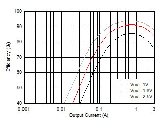
    1.     DC/DC 効率と出力電流との関係
  4. 改訂履歴
  5. 概要(続き)
  6. Pin Configuration and Functions
    1.     Pin Functions
  7. Specifications
    1. 7.1 Absolute Maximum Ratings
    2. 7.2 ESD Ratings
    3. 7.3 Recommended Operating Conditions
    4. 7.4 Thermal Information
    5. 7.5 Electrical Characteristics
    6. 7.6 I2C Serial Bus Timing Parameters
    7. 7.7 Typical Characteristics
  8. Detailed Description
    1. 8.1 Overview
    2. 8.2 Functional Block Diagram
    3. 8.3 Feature Description
      1. 8.3.1 DC/DC Converters
        1. 8.3.1.1 Overview
        2. 8.3.1.2 Transition Between PWM and PFM Modes
        3. 8.3.1.3 Buck Converter Load Current Measurement
        4. 8.3.1.4 Spread-Spectrum Mode
      2. 8.3.2 Sync Clock Functionality
      3. 8.3.3 Power-Up
      4. 8.3.4 Regulator Control
        1. 8.3.4.1 Enabling and Disabling Regulators
        2. 8.3.4.2 Changing Output Voltage
      5. 8.3.5 Enable and Disable Sequences
      6. 8.3.6 Device Reset Scenarios
      7. 8.3.7 Diagnosis and Protection Features
        1. 8.3.7.1 Power-Good Information (PGOOD pin)
          1. 8.3.7.1.1 PGOOD Pin Gated mode
          2. 8.3.7.1.2 PGOOD Pin Continuous Mode
        2. 8.3.7.2 Warnings for Diagnosis (Interrupt)
          1. 8.3.7.2.1 Output Power Limit
          2. 8.3.7.2.2 Thermal Warning
        3. 8.3.7.3 Protection (Regulator Disable)
          1. 8.3.7.3.1 Short-Circuit and Overload Protection
          2. 8.3.7.3.2 Overvoltage Protection
          3. 8.3.7.3.3 Thermal Shutdown
        4. 8.3.7.4 Fault (Power Down)
          1. 8.3.7.4.1 Undervoltage Lockout
      8. 8.3.8 Operation of the GPO Signals
      9. 8.3.9 Digital Signal Filtering
    4. 8.4 Device Functional Modes
      1. 8.4.1 Modes of Operation
    5. 8.5 Programming
      1. 8.5.1 I2C-Compatible Interface
        1. 8.5.1.1 Data Validity
        2. 8.5.1.2 Start and Stop Conditions
        3. 8.5.1.3 Transferring Data
        4. 8.5.1.4 I2C-Compatible Chip Address
        5. 8.5.1.5 Auto-Increment Feature
    6. 8.6 Register Maps
      1. 8.6.1 Register Descriptions
        1. 8.6.1.1  DEV_REV
        2. 8.6.1.2  OTP_REV
        3. 8.6.1.3  BUCK0_CTRL_1
        4. 8.6.1.4  BUCK0_CTRL_2
        5. 8.6.1.5  BUCK1_CTRL_1
        6. 8.6.1.6  BUCK1_CTRL_2
        7. 8.6.1.7  BUCK0_VOUT
        8. 8.6.1.8  BUCK1_VOUT
        9. 8.6.1.9  BUCK0_DELAY
        10. 8.6.1.10 BUCK1_DELAY
        11. 8.6.1.11 GPO_DELAY
        12. 8.6.1.12 GPO2_DELAY
        13. 8.6.1.13 GPO_CTRL
        14. 8.6.1.14 CONFIG
        15. 8.6.1.15 PLL_CTRL
        16. 8.6.1.16 PGOOD_CTRL_1
        17. 8.6.1.17 PGOOD_CTRL_2
        18. 8.6.1.18 PG_FAULT
        19. 8.6.1.19 RESET
        20. 8.6.1.20 INT_TOP_1
        21. 8.6.1.21 INT_TOP_2
        22. 8.6.1.22 INT_BUCK
        23. 8.6.1.23 TOP_STAT
        24. 8.6.1.24 BUCK_STAT
        25. 8.6.1.25 TOP_MASK_1
        26. 8.6.1.26 TOP_MASK_2
        27. 8.6.1.27 BUCK_MASK
        28. 8.6.1.28 SEL_I_LOAD
        29. 8.6.1.29 I_LOAD_2
        30. 8.6.1.30 I_LOAD_1
  9. Application and Implementation
    1. 9.1 Application Information
    2. 9.2 Typical Application
      1. 9.2.1 Design Requirements
        1. 9.2.1.1 Inductor Selection
        2. 9.2.1.2 Buck Input Capacitor Selection
        3. 9.2.1.3 Buck Output Capacitor Selection
      2. 9.2.2 Detailed Design Procedure
      3. 9.2.3 Application Curves
  10. 10Power Supply Recommendations
  11. 11Layout
    1. 11.1 Layout Guidelines
    2. 11.2 Layout Example
  12. 12デバイスおよびドキュメントのサポート
    1. 12.1 デバイス・サポート
      1. 12.1.1 デベロッパー・ネットワークの製品に関する免責事項
    2. 12.2 ドキュメントの更新通知を受け取る方法
    3. 12.3 コミュニティ・リソース
    4. 12.4 商標
    5. 12.5 静電気放電に関する注意事項
    6. 12.6 Glossary

パッケージ・オプション

メカニカル・データ(パッケージ|ピン)
サーマルパッド・メカニカル・データ
発注情報

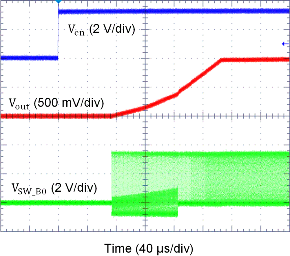
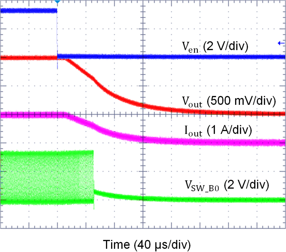
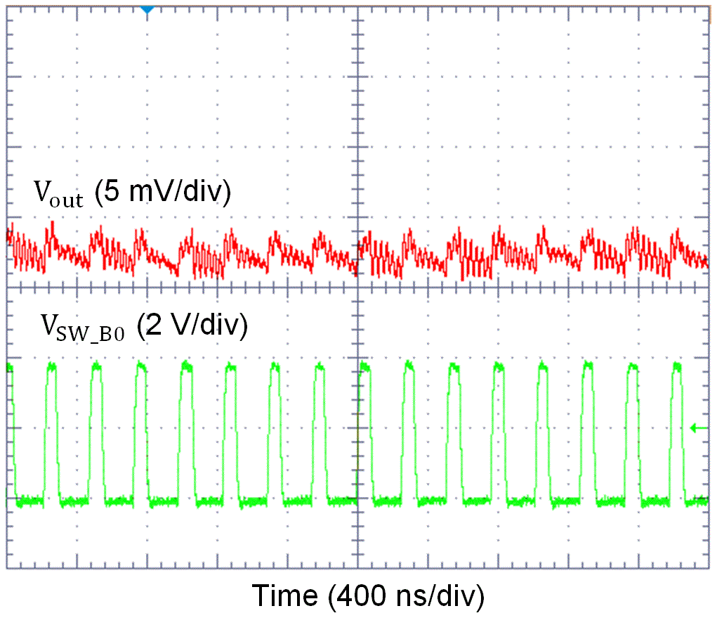
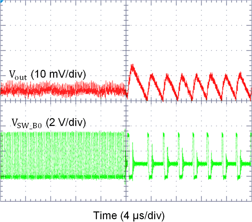
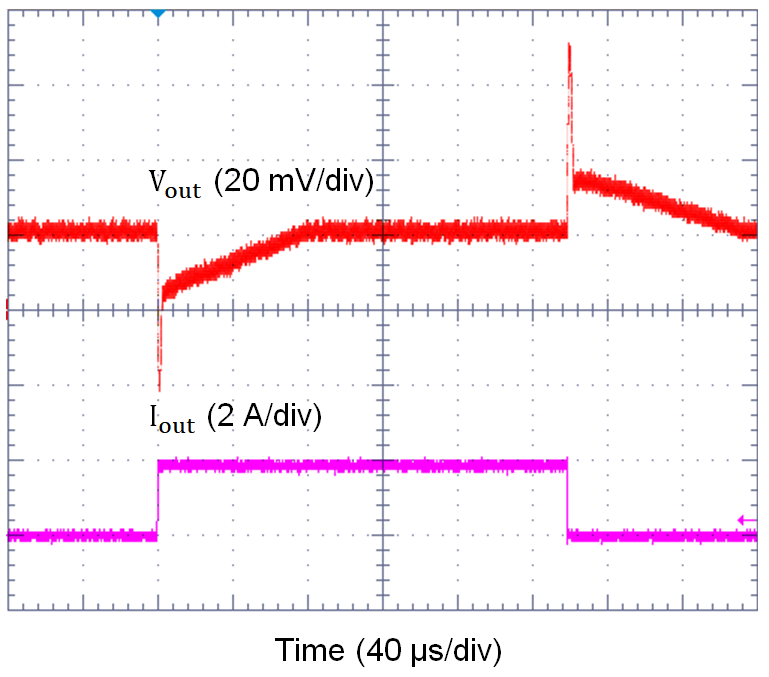
Application Curves

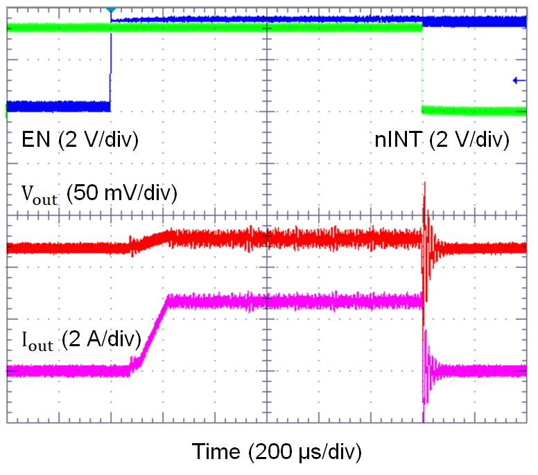
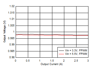
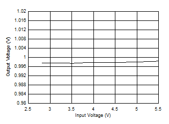
Measurements are done using typical application set up with connections shown in Figure 22. Graphs may not reflect the OTP default settings. Unless otherwise specified: V(VIN_Bx) = V(VANA) = 3.7 V, VOUT_Bx = 1 V, TA = 25°C, L = 0.47 µH (Murata DFE252012PD-R47M), COUT_BUCK = 22 µF, and CPOL_BUCK = 22 µF.
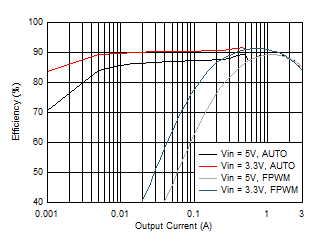
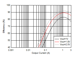
TPS65653-Q1 BUCK-efficiency-auto-vs-FPWM.gif
VOUT = 1.8 V
Figure 23. Buck Efficiency in PFM/PWM and Forced PWM Mode
TPS65653-Q1 BUCK-efficiency-FPWM-5Vin.gif
VIN = 5 V
Figure 25. Buck Efficiency in Forced PWM Mode
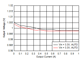
TPS65653-Q1 BUCK-output-voltage-vs-load-current-AUTO.gif
VOUT = 1 V
Figure 27. Buck Output Voltage vs Load Current in PFM/PWM Mode
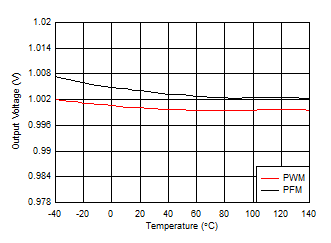
TPS65653-Q1 4mhz-vout-over-temp.gif
Load = 1 A (PWM) and 0.1 A (PFM)
Figure 29. Buck Output Voltage vs Temperature
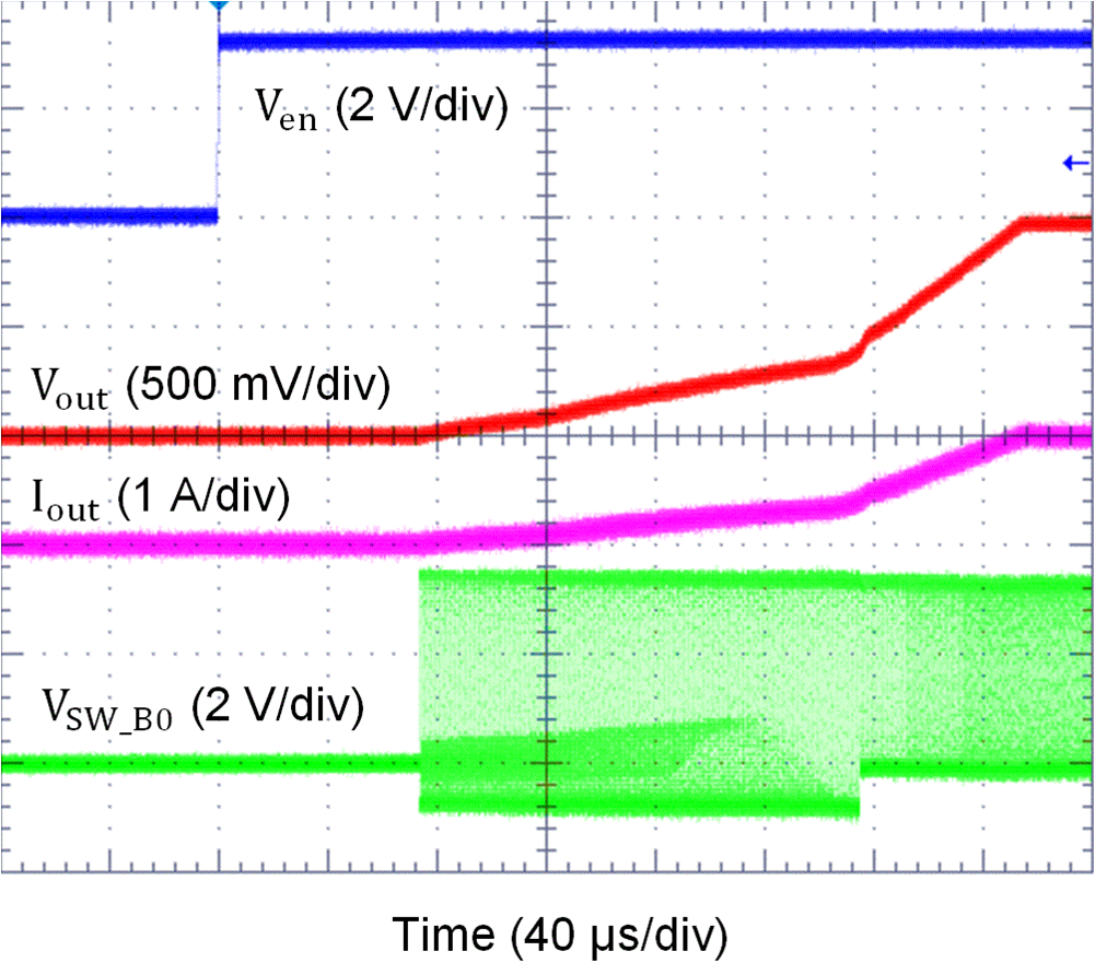
TPS65653-Q1 buck-startup-1a.png
Slew-rate = 10 mV/µs RLOAD = 1 Ω VOUT = 1 V
Figure 31. Buck Start-Up with EN1, Forced PWM Mode
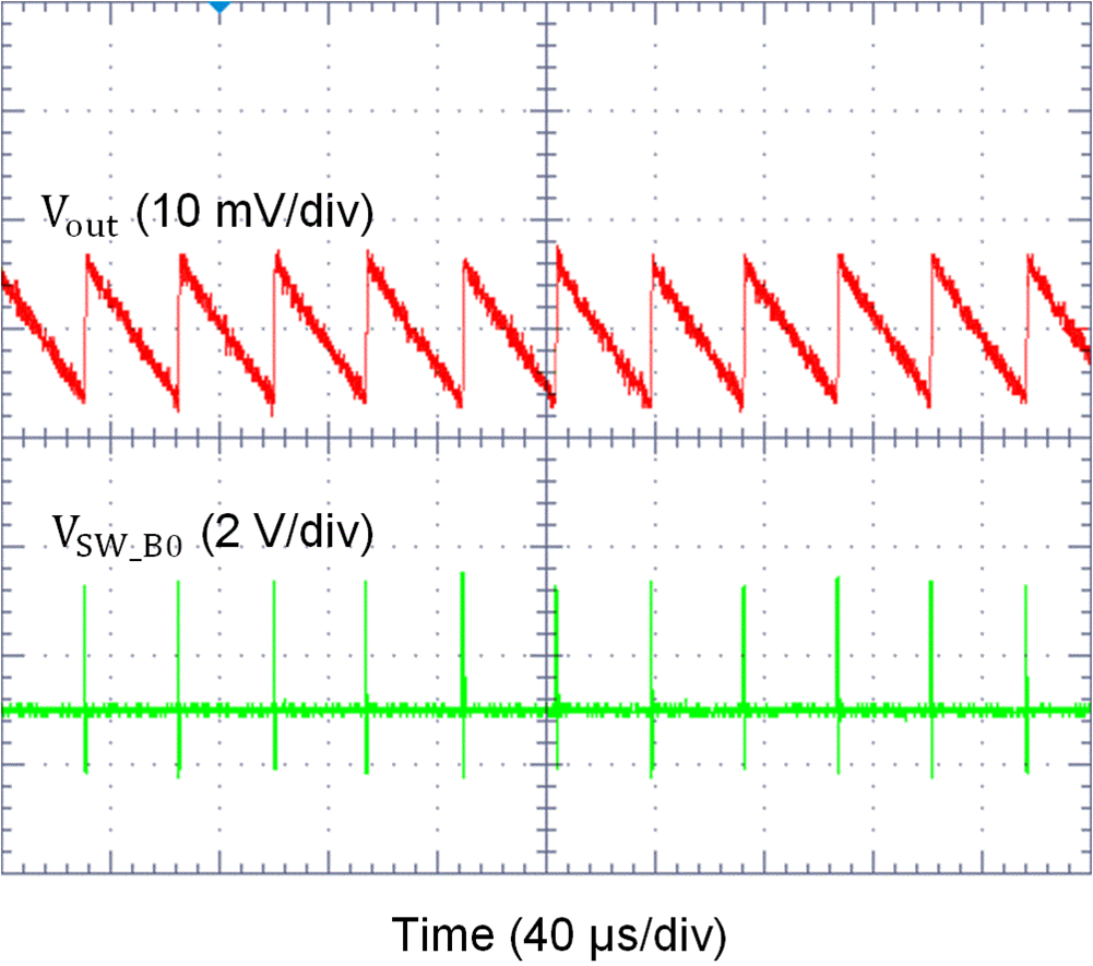
TPS65653-Q1 buck-pfm-ripple.png
IOUT = 10 mA
Figure 33. Buck Output Voltage Ripple, PFM Mode
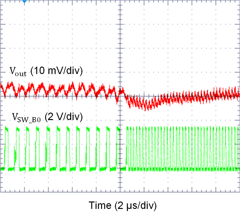
TPS65653-Q1 buck-pfm-to-pwm.png
Figure 35. Buck Transient From PFM-to-PWM Mode
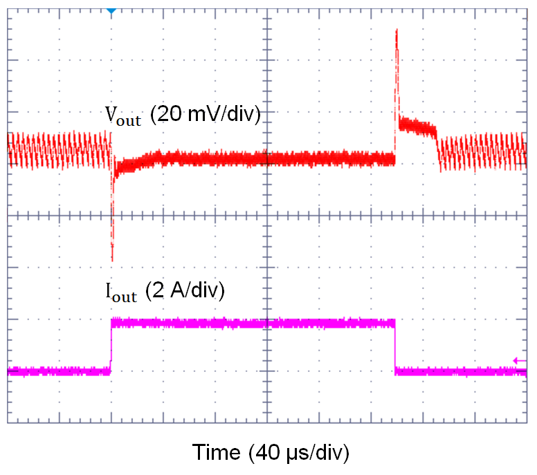
TPS65653-Q1 buck-transient-auto.png
IOUT = 0.1 A → 2 A → 0.1 A TR = TF = 400 ns
Figure 37. Buck Transient Load Step Response, AUTO Mode
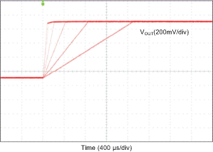
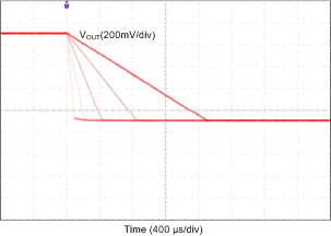
TPS65653-Q1 SNVSAB5_D046.gif
Figure 39. Buck VOUT Transition from 0.6 V to 1.4 V With Different Slew Rate Settings
TPS65653-Q1 buck-short.png
Figure 41. Buck Start-up With Short on Output
TPS65653-Q1 BUCK-efficiency-FPWM-3p3Vin.gif
VIN = 3.3 V
Figure 24. Buck Efficiency in Forced PWM Mode
TPS65653-Q1 BUCK-output-voltage-vs-load-current-FPWM.gif
VOUT = 1 V
Figure 26. Buck Output Voltage vs Load Current in Forced PWM Mode
TPS65653-Q1 BUCK-output-voltage-vs-input-voltage.gif
VOUT = 1 V Load = 1 A
Figure 28. Buck Output Voltage vs Input Voltage in PWM Mode
TPS65653-Q1 buck-startup-0a.png
Slew-rate = 10 mV/µs ILOAD = 0 A VOUT = 1 V
Figure 30. Buck Start-Up With EN1, Forced PWM Mode
TPS65653-Q1 buck-shutdown-1a.png
Slew-rate = 10 mV/µs RLOAD = 1 Ω VOUT = 1 V
Figure 32. Buck Shutdown With EN1, Forced PWM Mode
TPS65653-Q1 forced-pwm-ripple-500mA.gif
IOUT = 500 mA
Figure 34. Buck Output Voltage Ripple,
Forced PWM Mode
TPS65653-Q1 buck-pwm-to-pfm.png
Figure 36. Buck Transient From PWM-to-PFM Mode
TPS65653-Q1 buck-transient-pfm.png
IOUT = 0.1 A → 2 A → 0.1 A TR = TF = 400 ns
Figure 38. Buck Transient Load Step Response, Forced PWM Mode
TPS65653-Q1 SNVSAB5_D047.gif
Figure 40. Buck VOUT Transition from 1.4 V to 0.6 V With Different Slew Rate Settings