JAJSEM6J April 2006 – October 2020 TXB0104
PRODUCTION DATA
- 1 特長
- 2 アプリケーション
- 3 概要
- 4 Revision History
- 5 Pin Configuration and Functions
-
6 Specifications
- 6.1 Absolute Maximum Ratings
- 6.2 ESD Ratings
- 6.3 Recommended Operating Conditions
- 6.4 Thermal Information
- 6.5 Electrical Characteristics
- 6.6 Timing Requirements: VCCA = 1.2 V
- 6.7 Timing Requirements: VCCA = 1.5 V ± 0.1 V
- 6.8 Timing Requirements: VCCA = 1.8 V ± 0.15 V
- 6.9 Timing Requirements: VCCA = 2.5 V ± 0.2 V
- 6.10 Timing Requirements: VCCA = 3.3 V ± 0.3 V
- 6.11 Switching Characteristics: VCCA = 1.2 V
- 6.12 Switching Characteristics: VCCA = 1.5 V ± 0.1 V
- 6.13 Switching Characteristics: VCCA = 1.8 V ± 0.15 V
- 6.14 Switching Characteristics: VCCA = 2.5 V ± 0.2 V
- 6.15 Switching Characteristics: VCCA = 3.3 V ± 0.3 V
- 6.16 Operating Characteristics: VCCA = 1.2 V to 1.5 V, VCCB = 1.5 V to 1.8 V
- 6.17 Operating Characteristics: VCCA = 1.8 V to 3.3 V, VCCB = 1.8 V to 5 V
- 6.18 Typical Characteristics
- 7 Parameter Measurement Information
- 8 Detailed Description
- 9 Application and Implementation
- 10Power Supply Recommendations
- 11Layout
- 12Device and Documentation Support
- 13Mechanical, Packaging, and Orderable Information
パッケージ・オプション
デバイスごとのパッケージ図は、PDF版データシートをご参照ください。
メカニカル・データ(パッケージ|ピン)
- D|14
- RGY|14
- RUT|12
- NMN|12
- YZT|12
- PW|14
サーマルパッド・メカニカル・データ
発注情報
8.3.1 Architecture
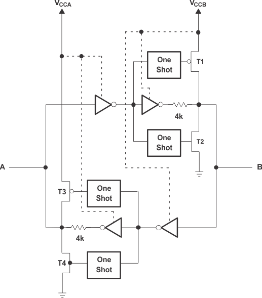
The TXB0104 device architecture (see Figure 8-1) does not require a direction-control signal to control the direction of data flow from A to B or from B to A. In a DC state, the output drivers of the device maintain a high or low, but are designed to be weak, so the output drivers can be overdriven by an external driver when data on the bus flows the opposite direction.
The output one-shots detect rising or falling edges on the A or B ports. During a rising edge, the one-shot turns on the PMOS transistors (T1, T3) for a short duration, which speeds up the low-to-high transition. Similarly, during a falling edge, the one-shot turns on the NMOS transistors (T2, T4) for a short duration, which speeds up the high-to-low transition. The typical output impedance during output transition is 70 Ω at VCCO = 1.2 V to 1.8 V, 50 Ω at VCCO = 1.8 V to 3.3 V, and 40 Ω at VCCO = 3.3 V to 5 V.
 Figure 8-1 Architecture of TXB0104 Device I/O Cell