JAJSEM6J April 2006 – October 2020 TXB0104
PRODUCTION DATA
- 1 特長
- 2 アプリケーション
- 3 概要
- 4 Revision History
- 5 Pin Configuration and Functions
-
6 Specifications
- 6.1 Absolute Maximum Ratings
- 6.2 ESD Ratings
- 6.3 Recommended Operating Conditions
- 6.4 Thermal Information
- 6.5 Electrical Characteristics
- 6.6 Timing Requirements: VCCA = 1.2 V
- 6.7 Timing Requirements: VCCA = 1.5 V ± 0.1 V
- 6.8 Timing Requirements: VCCA = 1.8 V ± 0.15 V
- 6.9 Timing Requirements: VCCA = 2.5 V ± 0.2 V
- 6.10 Timing Requirements: VCCA = 3.3 V ± 0.3 V
- 6.11 Switching Characteristics: VCCA = 1.2 V
- 6.12 Switching Characteristics: VCCA = 1.5 V ± 0.1 V
- 6.13 Switching Characteristics: VCCA = 1.8 V ± 0.15 V
- 6.14 Switching Characteristics: VCCA = 2.5 V ± 0.2 V
- 6.15 Switching Characteristics: VCCA = 3.3 V ± 0.3 V
- 6.16 Operating Characteristics: VCCA = 1.2 V to 1.5 V, VCCB = 1.5 V to 1.8 V
- 6.17 Operating Characteristics: VCCA = 1.8 V to 3.3 V, VCCB = 1.8 V to 5 V
- 6.18 Typical Characteristics
- 7 Parameter Measurement Information
- 8 Detailed Description
- 9 Application and Implementation
- 10Power Supply Recommendations
- 11Layout
- 12Device and Documentation Support
- 13Mechanical, Packaging, and Orderable Information
パッケージ・オプション
デバイスごとのパッケージ図は、PDF版データシートをご参照ください。
メカニカル・データ(パッケージ|ピン)
- D|14
- RGY|14
- RUT|12
- NMN|12
- YZT|12
- PW|14
サーマルパッド・メカニカル・データ
発注情報
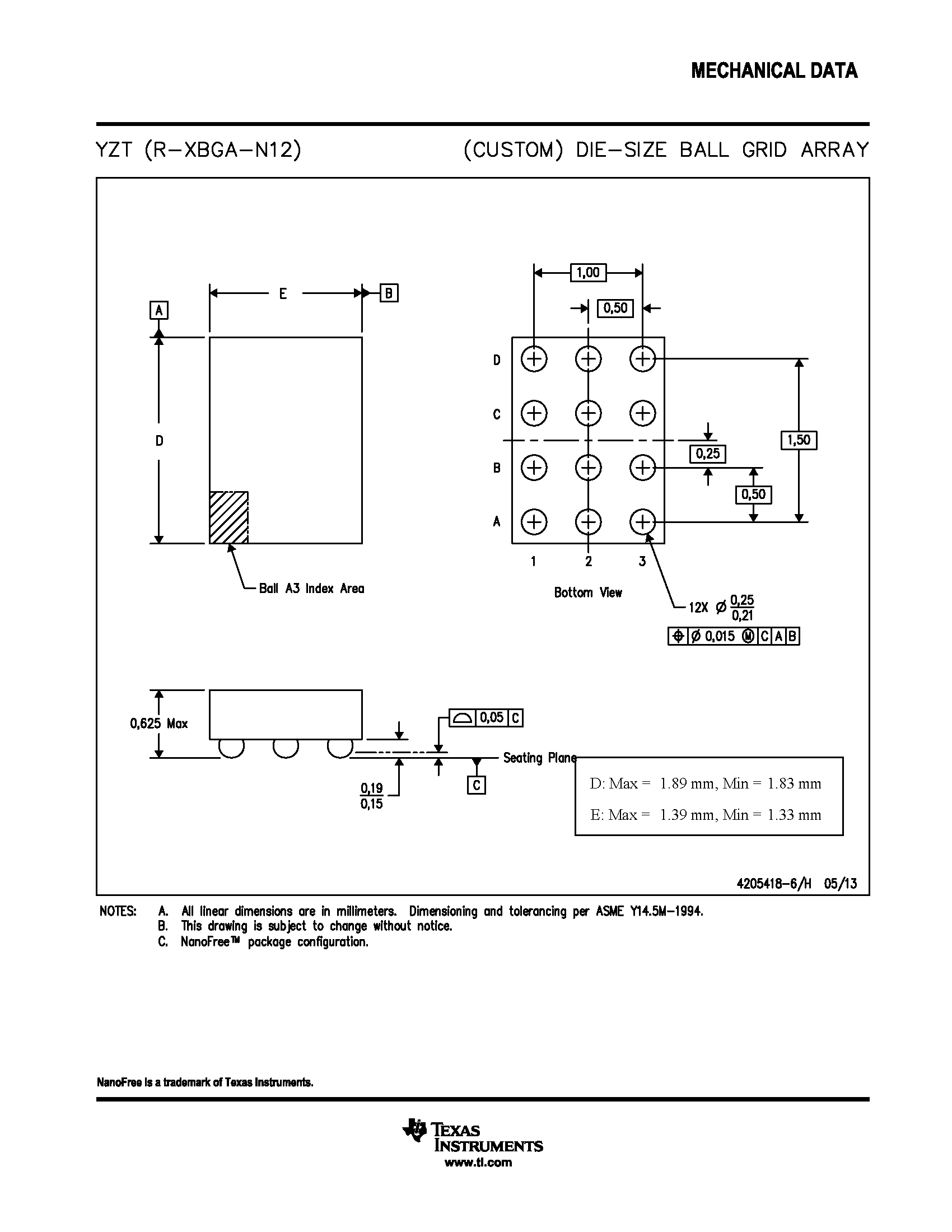
13 Mechanical, Packaging, and Orderable Information
The following pages include mechanical, packaging, and orderable information. This information is the most current data available for the designated devices. This data is subject to change without notice and revision of this document. For browser-based versions of this data sheet, refer to the left-hand navigation.