SBAU378A September 2021 – January 2022 ADS1148 , ADS1248
- Trademarks
- 1Introduction
- 2Getting Started With the ADS1x48EVM
-
3ADS1x48EVM Overview
- 3.1 Analog and Digital Power Supplies
- 3.2 Voltage Reference Options
- 3.3 Clock Options
- 3.4 Digital Interface
- 3.5
Analog Input Connections
- 3.5.1 Connecting a Thermocouple to J5 on the ADS1x48EVM
- 3.5.2 Connecting a Thermistor to J5 on the ADS1x48EVM
- 3.5.3
Connecting an RTD to J6 on the ADS1x48EVM
- 3.5.3.1 Connecting a 2-Wire RTD Using a Low-Side RREF to J6 on the ADS1x48EVM
- 3.5.3.2 Connecting a 2-Wire RTD Using a High-Side RREF to J6 on the ADS1x48EVM
- 3.5.3.3 Connecting a 3-Wire RTD Using One IDAC and a Low-Side RREF to J6 on the ADS1x48EVM
- 3.5.3.4 Connecting a 3-Wire RTD Using One IDAC and a High-Side RREF to J6 on the ADS1x48EVM
- 3.5.3.5 Connecting a 3-Wire RTD Using Two IDACs and a Low-Side RREF to J6 on the ADS1x48EVM
- 3.5.3.6 Connecting a 3-Wire RTD Using Two IDACs and a High-Side RREF to J6 on the ADS1x48EVM
- 3.5.3.7 Connecting a 4-Wire RTD Using a Low-Side RREF to J6 on the ADS1x48EVM
- 3.5.3.8 Connecting a 4-Wire RTD Using a High-Side RREF to J6 on the ADS1x48EVM
- 3.5.3.9 Summary of ADS1x48EVM RTD Configuration Settings
- 3.5.4 Connecting a General-Purpose Input to J5 on the ADS1x48EVM
- 4ADS1x48EVM GUI
- 5Bill of Materials, Printed Circuit Board Layout, and Schematic
- 6Revision History
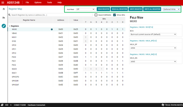
4.3.1 Register Read and Write Options
Figure 4-11 highlights the top of the Register Map window where reading from and writing to registers is controlled. The default behavior has the Auto Read register function turned off as well as performs an Immediately Write operation on the Config register when options change. All read and write options are discussed in more detail in the next sections.
 Figure 4-11 Register Read and Write Controls