SBAU378A September 2021 – January 2022 ADS1148 , ADS1248
- Trademarks
- 1Introduction
- 2Getting Started With the ADS1x48EVM
-
3ADS1x48EVM Overview
- 3.1 Analog and Digital Power Supplies
- 3.2 Voltage Reference Options
- 3.3 Clock Options
- 3.4 Digital Interface
- 3.5
Analog Input Connections
- 3.5.1 Connecting a Thermocouple to J5 on the ADS1x48EVM
- 3.5.2 Connecting a Thermistor to J5 on the ADS1x48EVM
- 3.5.3
Connecting an RTD to J6 on the ADS1x48EVM
- 3.5.3.1 Connecting a 2-Wire RTD Using a Low-Side RREF to J6 on the ADS1x48EVM
- 3.5.3.2 Connecting a 2-Wire RTD Using a High-Side RREF to J6 on the ADS1x48EVM
- 3.5.3.3 Connecting a 3-Wire RTD Using One IDAC and a Low-Side RREF to J6 on the ADS1x48EVM
- 3.5.3.4 Connecting a 3-Wire RTD Using One IDAC and a High-Side RREF to J6 on the ADS1x48EVM
- 3.5.3.5 Connecting a 3-Wire RTD Using Two IDACs and a Low-Side RREF to J6 on the ADS1x48EVM
- 3.5.3.6 Connecting a 3-Wire RTD Using Two IDACs and a High-Side RREF to J6 on the ADS1x48EVM
- 3.5.3.7 Connecting a 4-Wire RTD Using a Low-Side RREF to J6 on the ADS1x48EVM
- 3.5.3.8 Connecting a 4-Wire RTD Using a High-Side RREF to J6 on the ADS1x48EVM
- 3.5.3.9 Summary of ADS1x48EVM RTD Configuration Settings
- 3.5.4 Connecting a General-Purpose Input to J5 on the ADS1x48EVM
- 4ADS1x48EVM GUI
- 5Bill of Materials, Printed Circuit Board Layout, and Schematic
- 6Revision History
4.3 Register Map
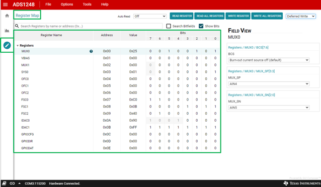
The Register Map window contains information about the how the ADS1x48 is configured. A number of control buttons and drop-down menus exist to configure the Register Map read and write operations.
Throughout the Register Map window question mark icons appear. Clicking on these icons provides details pertaining to the items in the locations where they appear. See Figure 4-10 for more details.
 Figure 4-10 Register Map
As shown in Figure 4-10, the ADS1x48 devices have many configurable registers. Configure these registers by using the drop-down menu and clickable options shown in the Field View menu on the right side of the GUI window. The Field View menu replicates the register setting information provided in the ADS1x48 data sheets. Reference these documents for additional information about or questions related to the specific ADC register settings.
Instead of using the Field View menu, the 1's and 0's can also be double-clicked in the Bits menu to toggle the bit settings. As the bit settings change, the Field View options also change to the corresponding register setting.