SBOU024C august 2004 – july 2023 PGA309
- 1
- Read This First
-
1Introduction
- 1.1 PGA309 Functional Description
- 1.2 Sensor Error Adjustment Range
- 1.3 Gain Scaling
- 1.4 Offset Adjustment
- 1.5 Voltage Reference
- 1.6 Sensor Excitation and Linearization
- 1.7 ADC for Temperature Sensing
- 1.8 External EEPROM and Temperature Coefficients
- 1.9 Fault Monitor
- 1.10 Over-Scale and Under-Scale Limits
- 1.11 Power-Up and Normal Operation
- 1.12 Digital Interface
- 1.13 Pin Configuration
- 2Detailed Description
- 3Operating Modes
-
4Digital Interface
- 4.1 Description
- 4.2 Two-Wire Interface
- 4.3 One-Wire Interface
- 4.4 One-Wire Interface Timeout
- 4.5 One-Wire Interface Timing Considerations
- 4.6 Two-Wire Access to External EEPROM
- 4.7 One-Wire Interface Initiated Two-Wire EEPROM Transactions
- 4.8 PGA309 Stand-Alone Mode and Two-Wire Transactions
- 4.9 PGA309 Two-Wire Bus Master Operation and Bus Sharing Considerations
- 4.10 One-Wire Operation with PRG Connected to VOUT
- 4.11 Four-Wire Modules and One-Wire Interface (PRG)
- 5Application Background
-
6Register Descriptions
- 6.1 Internal Register Overview
- 6.2
Internal Register Map
- 6.2.1 Register 0: Temp ADC Output Register (Read Only, Address Pointer = 00000)
- 6.2.2 Register 1: Fine Offset Adjust (Zero DAC) Register (Read/Write, Address Pointer = 00001)
- 6.2.3 Register 2: Fine Gain Adjust (Gain DAC) Register (Read/Write, Address Pointer = 00010)
- 6.2.4 Register 3: Reference Control and Linearization Register (Read/Write, Address Pointer = 00011)
- 6.2.5 Register 4: PGA Coarse Offset Adjust and Gain Select/Output Amplifier Gain Select Register (Read/Write, Address Pointer = 00100)
- 6.2.6 Register 5: PGA Configuration and Over/Under-Scale Limit Register (Read/Write, Address Pointer = 00101)
- 6.2.7 Register 6: Temp ADC Control Register (Read/Write, Address Pointer = 00110)
- 6.2.8 Register 7: Output Enable Counter Control Register (Read/Write, Address Pointer = 00111)
- 6.2.9 Register 8: Alarm Status Register (Read Only, Address Pointer = 01000)
- A External EEPROM Example
- B Detailed Block Diagram
- C Glossary
- Revision History
2.6 Linearization Function
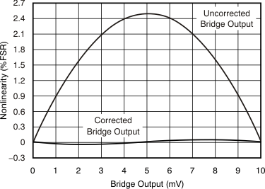
Many bridge sensors have an inherently nonlinear output with applied pressure. Figure 2-9 illustrates a typical nonlinearity correction using the PGA309 linearization circuit.
 Figure 2-9 Bridge Pressure Nonlinearity Correction
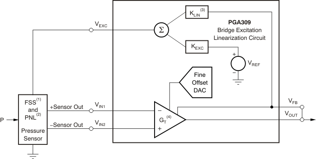
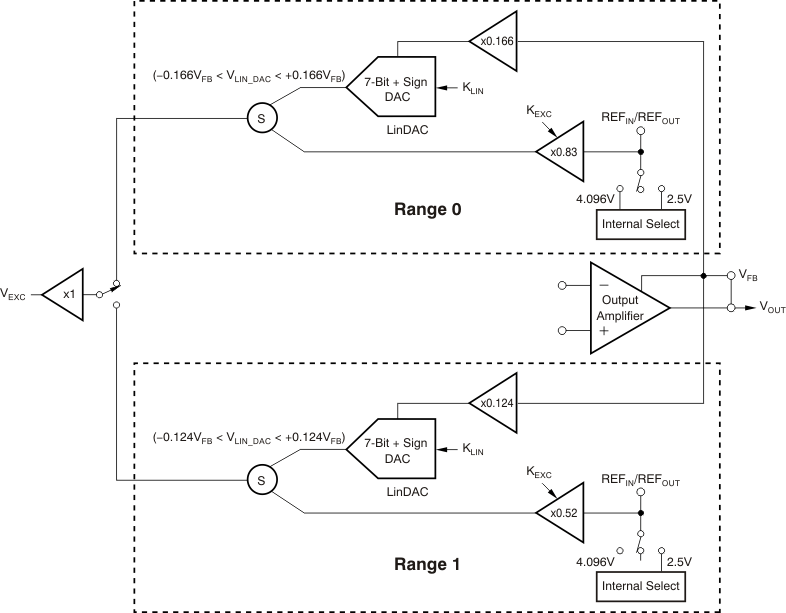
The PGA309 contains a dedicated circuit for sensor voltage excitation and linearization, as shown in Figure 2-10. The Linearization Circuit scales the selected VREF and sums it together with a portion of the output voltage (VOUT) through the feedback pin (VFB) to compensate for the bow-shaped nonlinearity of the bridge sensor output versus pressure. Using this technique, it is possible to compensate for parabolic nonlinearity resulting in up to a 20:1 improvement over an uncompensated bridge output, as shown in Figure 2-9. KLIN is a bipolar scale factor of VOUT produced by the Lin DAC. KEXC is a set attenuation factor of VREF to allow for increases or decreases to VEXC, as required. There are two ranges available in the Linearization Circuit, with a different respective range and a different respective fixed attenuation for KLIN.

- FSS = Full-Scale bridge Sensitivity of sensor.
- PNL = Pressure Nonlinearity of sensor.
- KLIN = Linearization coefficient set by the Lin DAC.
- GT = (Front-End PGA Gain)(Gain DAC)(Output Amplifier Gain).
If no sensor voltage excitation linearization is needed, there are several options for the bridge excitation. In ratiometric systems, the bridge should be tied directly to VSA. In systems that provide an external reference for VREF, the sensor should be tied to this external sensor. For systems that use the PGA309 internal reference, it is recommended that VEXC be used for sensor excitation, and Lin DAC be set to zero. The reason for this is to minimize any large current draws from the REFIN/REFOUT pin that could affect the internal VREF value used by the internal circuits.
In systems that do not use VEXC, both the Lin DAC and VEXC may be disabled by setting the appropriate Register 3 bits (10, 7:0) to ‘0’. This results in 50μA to 100μA of lower total quiescent current.
The typical bandwidth of the Linearization Circuit from the VFB pin to VEXC is 35kHz.
The output signal-dependence (VOUT dependence) of the bridge excitation (VEXC) adds a second-order term to the overall system transfer function (PGA309 + bridge sensor). The Lin DAC shown in Figure 2-11 scales a portion of VOUT that is then summed with a scaled version of the reference voltage, VREF. The Lin DAC code can be set to compensate for each individual bridge sensor nonlinearity. As illustrated in Figure 2-11, there are two ranges available in the PGA309 Linearization Circuit to accommodate a variety of sensor nonlinearities and VREF combinations.
 Figure 2-11 Linearization Circuit
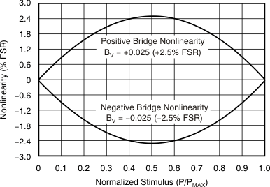
To determine the value for the Lin DAC, also called the linearization coefficient KLIN, the nonlinearity of the bridge sensor with constant excitation voltage must be known. The PGA309 linearization circuitry can only compensate for the parabolic-shaped portions of a sensor’s nonlinearity with applied pressure. This nonlinearity is assumed to be constant over temperature or the temperature variations are assumed to be an insignificant contribution to the system error budget. For the typical PGA309 application, the KLIN factor is not adjusted with temperature changes. Optimum correction occurs when maximum deviation from a linear output occurs at mid-scale, as shown in Figure 2-12 and Figure 2-13. Sensors with nonlinearity curves similar to that of Figure 2-12, but not peaking at exactly mid-scale, can still be substantially improved. A sensor with an S-shaped nonlinearity curve (equal positive and negative nonlinearity) cannot be improved by using the PGA309 Linearization Circuit.
 Figure 2-12 Bridge Output vs Pressure
 Figure 2-13 Bridge Nonlinearity (%FSR) vs Pressure
Either positive or negative bridge nonlinearities can be compensated by the proper setting of the Lin DAC polarity. To correct for positive bridge nonlinearity (upward bowing—shown in Figure 2-13), the Lin DAC value should be set positive. For negative bridge nonlinearity (downward bowing—shown in Figure 2-13), set the Lin DAC value negative.
The excitation voltage (VEXC) directly scales the bridge sensor output, and therefore, must be accounted for in the gain and offset setting of the PGA309 when the linearization circuit is used.
Key definitions and design equations for the linearization circuit are given in the following sections.