SBOU024C august 2004 – july 2023 PGA309
- 1
- Read This First
-
1Introduction
- 1.1 PGA309 Functional Description
- 1.2 Sensor Error Adjustment Range
- 1.3 Gain Scaling
- 1.4 Offset Adjustment
- 1.5 Voltage Reference
- 1.6 Sensor Excitation and Linearization
- 1.7 ADC for Temperature Sensing
- 1.8 External EEPROM and Temperature Coefficients
- 1.9 Fault Monitor
- 1.10 Over-Scale and Under-Scale Limits
- 1.11 Power-Up and Normal Operation
- 1.12 Digital Interface
- 1.13 Pin Configuration
- 2Detailed Description
- 3Operating Modes
-
4Digital Interface
- 4.1 Description
- 4.2 Two-Wire Interface
- 4.3 One-Wire Interface
- 4.4 One-Wire Interface Timeout
- 4.5 One-Wire Interface Timing Considerations
- 4.6 Two-Wire Access to External EEPROM
- 4.7 One-Wire Interface Initiated Two-Wire EEPROM Transactions
- 4.8 PGA309 Stand-Alone Mode and Two-Wire Transactions
- 4.9 PGA309 Two-Wire Bus Master Operation and Bus Sharing Considerations
- 4.10 One-Wire Operation with PRG Connected to VOUT
- 4.11 Four-Wire Modules and One-Wire Interface (PRG)
- 5Application Background
-
6Register Descriptions
- 6.1 Internal Register Overview
- 6.2
Internal Register Map
- 6.2.1 Register 0: Temp ADC Output Register (Read Only, Address Pointer = 00000)
- 6.2.2 Register 1: Fine Offset Adjust (Zero DAC) Register (Read/Write, Address Pointer = 00001)
- 6.2.3 Register 2: Fine Gain Adjust (Gain DAC) Register (Read/Write, Address Pointer = 00010)
- 6.2.4 Register 3: Reference Control and Linearization Register (Read/Write, Address Pointer = 00011)
- 6.2.5 Register 4: PGA Coarse Offset Adjust and Gain Select/Output Amplifier Gain Select Register (Read/Write, Address Pointer = 00100)
- 6.2.6 Register 5: PGA Configuration and Over/Under-Scale Limit Register (Read/Write, Address Pointer = 00101)
- 6.2.7 Register 6: Temp ADC Control Register (Read/Write, Address Pointer = 00110)
- 6.2.8 Register 7: Output Enable Counter Control Register (Read/Write, Address Pointer = 00111)
- 6.2.9 Register 8: Alarm Status Register (Read Only, Address Pointer = 01000)
- A External EEPROM Example
- B Detailed Block Diagram
- C Glossary
- Revision History
2.11 General AC Considerations
In addition to normal good analog layout and design practices, there are a few key items to check when designing with the PGA309.
- REFIN/REFOUT, pin 16: Keep capacitive loading to 200pF or less.
- VEXC, pin 1: Keep capacitive loading to 200pF or less.
- VSA, pin 3 and VSD, pin 10: Keep these within 200mV of each other. Internally, the PGA309 separates its digital and analog power supplies to minimize cross-talk between the two. Externally, tie the two together and bypass, directly at the pins, with a 0.1μF capacitor. If an RC filter is used between the two supplies, ensure that maximum drop is never more than 200mV.
- GNDA, pin 2 and GNDD, pin11: Ensure that these are both tied directly together and connected to the same ground point.
- VSJ, pin 8: This is the negative input to the Output Amplifier and as such, it is high-impedance. Route low-impedance traces, such as VOUT, and noisy traces away from VSJ. Minimize trace lengths to avoid unwanted additional capacitance on VSJ.
- VIN1, pin 4 and VIN2, pin 5: For source resistances greater than or equal to 10kΩ, add a capacitor of 1nF to 2nF between VIN1 and VIN2 to minimize noise coupling.
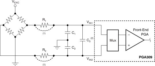
- VIN1, pin 4 and VIN2, pin 5: RFI filtering is always a concern for instrumentation amplifier applications. RFI signals injected into instrumentation amplifiers become rectified and appear on the output as a DC drift or offset; high-gain circuits amplify this effect. Figure 2-39 depicts input filtering for the PGA309. Depending upon the distance of the bridge sensor from the PGA309 and the sensor module shielding, R1 and R2 may be required. C1 should be equal to C2, and C3 should be ten times larger than C1 to attenuate any common-mode signals that become differential due to the mismatch in C1 and C2. All input filter components should be located directly at the PGA309 inputs to avoid and trace lengths from becoming receiving RFI antennas.
 Figure 2-39 Input Filtering