SBOU024C august 2004 – july 2023 PGA309
- 1
- Read This First
-
1Introduction
- 1.1 PGA309 Functional Description
- 1.2 Sensor Error Adjustment Range
- 1.3 Gain Scaling
- 1.4 Offset Adjustment
- 1.5 Voltage Reference
- 1.6 Sensor Excitation and Linearization
- 1.7 ADC for Temperature Sensing
- 1.8 External EEPROM and Temperature Coefficients
- 1.9 Fault Monitor
- 1.10 Over-Scale and Under-Scale Limits
- 1.11 Power-Up and Normal Operation
- 1.12 Digital Interface
- 1.13 Pin Configuration
- 2Detailed Description
- 3Operating Modes
-
4Digital Interface
- 4.1 Description
- 4.2 Two-Wire Interface
- 4.3 One-Wire Interface
- 4.4 One-Wire Interface Timeout
- 4.5 One-Wire Interface Timing Considerations
- 4.6 Two-Wire Access to External EEPROM
- 4.7 One-Wire Interface Initiated Two-Wire EEPROM Transactions
- 4.8 PGA309 Stand-Alone Mode and Two-Wire Transactions
- 4.9 PGA309 Two-Wire Bus Master Operation and Bus Sharing Considerations
- 4.10 One-Wire Operation with PRG Connected to VOUT
- 4.11 Four-Wire Modules and One-Wire Interface (PRG)
- 5Application Background
-
6Register Descriptions
- 6.1 Internal Register Overview
- 6.2
Internal Register Map
- 6.2.1 Register 0: Temp ADC Output Register (Read Only, Address Pointer = 00000)
- 6.2.2 Register 1: Fine Offset Adjust (Zero DAC) Register (Read/Write, Address Pointer = 00001)
- 6.2.3 Register 2: Fine Gain Adjust (Gain DAC) Register (Read/Write, Address Pointer = 00010)
- 6.2.4 Register 3: Reference Control and Linearization Register (Read/Write, Address Pointer = 00011)
- 6.2.5 Register 4: PGA Coarse Offset Adjust and Gain Select/Output Amplifier Gain Select Register (Read/Write, Address Pointer = 00100)
- 6.2.6 Register 5: PGA Configuration and Over/Under-Scale Limit Register (Read/Write, Address Pointer = 00101)
- 6.2.7 Register 6: Temp ADC Control Register (Read/Write, Address Pointer = 00110)
- 6.2.8 Register 7: Output Enable Counter Control Register (Read/Write, Address Pointer = 00111)
- 6.2.9 Register 8: Alarm Status Register (Read Only, Address Pointer = 01000)
- A External EEPROM Example
- B Detailed Block Diagram
- C Glossary
- Revision History
4.11 Four-Wire Modules and One-Wire Interface (PRG)
In four-wire module applications, it is essential that the OWD Bit (Register 4 [D15]) be set to '1' to disable the One-Wire interface after final programming is complete and before the final sensor module is sent out to the end application. In a four-terminal module, the PRG pin is connected directly to the outside world and is even more susceptible to noise coupled into it from periodic noise generators. Repetitive noise, such as a commutating motor or a switching power supply, can cause the PRG circuitry to misinterpret this noise as valid communication and put the PGA309 into an unpredicted state or, worse, cause EEPROM corruption.
Even if the OWD bit is set to '1' to disable the One-Wire interface, a 33ms window remains open on power-up, where periodic noise can be coupled into the PRG pin and be interpreted as coherent communication. The four-terminal module application, as show in Figure 4-17, requires detailed discussion and consideration when bringing the PRG pin directly to the outside world.
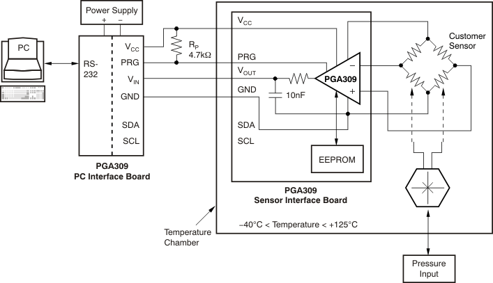 Figure 4-17 Four-Wire Sensor Module Application
Figure 4-20 depicts details of the PRG circuitry within the PGA309. Additional external protection components and electromagnetic interferences/radio frequency interference (EMI/RFI) filtering are included in this discussion. Considerations for programming the PGA309 four-terminal sensor module are presented with reference to Figure 4-20.
The PGA309 contains electrostatic discharge (ESD) cells, D2 and D1/SCR1, on the PRG pin to prevent ESD damage when the device is being handled before installation on a printed circuit board. These same ESD cells may not be adequate when the PGA309 is installed in a complete circuit with regards to electrical overstress. The ESD diodes D1 and D2 can handle up to 10mA continuous load. However, SCR1 will trigger with a 14V level and then drop to 3V at 80mA of sustaining current, as Figure 4-18 shows. If the current is not limited, the voltage will increase again; this increase, combined with higher currents, may cause permanent damage to the ESD cells and make the PRG circuitry unusable.
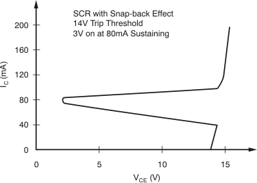 Figure 4-18 SCR ESD Cell
If miswiring is or external electrical overstresses are anticipated, the PRG pin must be protected by using external devices. SD1 and SD2 are signal Schottky diodes that steer current away from the internal ESD cells on the PRG pin during electrical overstress events. R7 will limit the current through SD1 and SD2. Z1 is a zener diode to clamp the energy passed through SD1. The selection of R7 can impact the valid logic levels at PRG_PGA309 and PRG_ Programmer. SW1 and RON represent the MOSFET switch and on-resistance used on the PGA309EVM or customer programmer that configures and calibrates the PGA309 over the One-Wire interface. For the PGA309, logic high is 0.7VSD (3.5V for VSD = 5V) or greater; logic low is 0.2VSD (1V for VSD = 5V) or less. Logic high is not a concern because there are pull-up resistors on the PGA309 module and on the programmer. The worst-case condition for logic low is shown in Figure 4-20; this figure illustrates the condition at approximately 610mV, which is less than the specified 0.2VSD (1V for VSD = 5V) maximum logic low. This configuration will be adequate for up to ±50V of miswiring on the 1W pin, based on current flow and the power dissipation of the components shown up to a temperature of +75°C.
Each individual application should be analyzed for electrical overstress and proper programming logic levels on the PRG pin.
Refer to Figure 4-21 for an illustration of common EMI/RFI filtering and the PRG pin configuration. Most EMI/RFI filter schemes typically involve connecting the chassis ground to the signal ground via capacitors in the range of 1nF to 10nF. These capacitors are connected on every pin into and out of the module. In Figure 4-21, we connect the signal ground to the chassis ground with capacitor C2 (1nF). VCC is connected to the chassis ground through capacitor C4 (100nF) and capacitor C2 (1nF). We also add capacitor C1 (10nF) from the PRG pin at the module output and tie it directly to VCC. This configuration is optimal for rejecting any switching disturbances between the chassis ground and the signal ground.
EMI/RFI is often seen as disturbance referenced to the chassis ground, as shown in Figure 4-19. A common source impedance of 50Ω (through R11) is assumed. The disturbance is injected into the PRG pin of the module, and will then flow through capacitors C3 (10nF), C4 (100nF), and C2 (1nF) as it returns to chassis ground. A severe disturbance of ±5V at 100kHz will only degrade the logic high voltage on the PRG pin from 5V to 4.27V, as shown in Figure 5-4. The minimum logic high is 0.7VSD (3.5V for VSD = 5V) , and thus there will be no PRG miscommunication caused by this severe disturbance between chassis ground and signal ground.
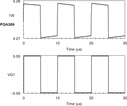 Figure 4-19 Severe EMI/RFI Disturbance
As a final note, consider Figure 4-20 once more, and observe that in order to program a PRG pin on a module with large capacitance (for example, with C1 = 10nF) on the PRG pin, the customer programmer must use a PRG speed-up circuit, which detects a rising edge on the PRG signal. Based on this rising edge, a switch connects the PRG line to +5V through a 200Ω resistor for 5μs in order to quickly charge capacitor C1 (10nF) and obtain a reasonable rising edge in logic '0' to logic '1' transitions. The PGA309EVM has this PRG speed-up circuit already installed in the PC Programmer Interface Board.
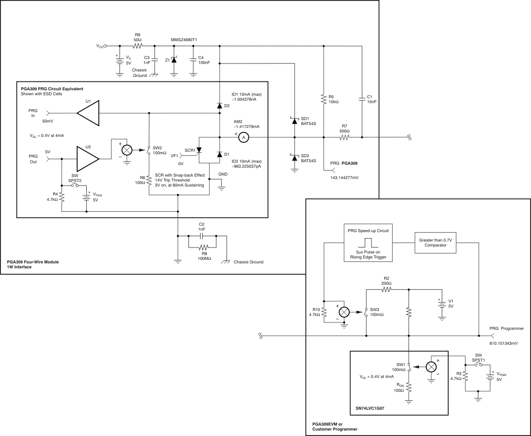 Figure 4-20 PRG Circuit Protection Logic Levels
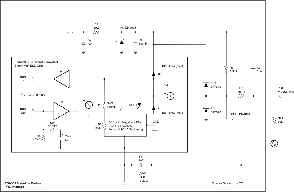 Figure 4-21 PRG Circuit EMI/RFI Filtering