SBOU024C august 2004 – july 2023 PGA309
- 1
- Read This First
-
1Introduction
- 1.1 PGA309 Functional Description
- 1.2 Sensor Error Adjustment Range
- 1.3 Gain Scaling
- 1.4 Offset Adjustment
- 1.5 Voltage Reference
- 1.6 Sensor Excitation and Linearization
- 1.7 ADC for Temperature Sensing
- 1.8 External EEPROM and Temperature Coefficients
- 1.9 Fault Monitor
- 1.10 Over-Scale and Under-Scale Limits
- 1.11 Power-Up and Normal Operation
- 1.12 Digital Interface
- 1.13 Pin Configuration
- 2Detailed Description
- 3Operating Modes
-
4Digital Interface
- 4.1 Description
- 4.2 Two-Wire Interface
- 4.3 One-Wire Interface
- 4.4 One-Wire Interface Timeout
- 4.5 One-Wire Interface Timing Considerations
- 4.6 Two-Wire Access to External EEPROM
- 4.7 One-Wire Interface Initiated Two-Wire EEPROM Transactions
- 4.8 PGA309 Stand-Alone Mode and Two-Wire Transactions
- 4.9 PGA309 Two-Wire Bus Master Operation and Bus Sharing Considerations
- 4.10 One-Wire Operation with PRG Connected to VOUT
- 4.11 Four-Wire Modules and One-Wire Interface (PRG)
- 5Application Background
-
6Register Descriptions
- 6.1 Internal Register Overview
- 6.2
Internal Register Map
- 6.2.1 Register 0: Temp ADC Output Register (Read Only, Address Pointer = 00000)
- 6.2.2 Register 1: Fine Offset Adjust (Zero DAC) Register (Read/Write, Address Pointer = 00001)
- 6.2.3 Register 2: Fine Gain Adjust (Gain DAC) Register (Read/Write, Address Pointer = 00010)
- 6.2.4 Register 3: Reference Control and Linearization Register (Read/Write, Address Pointer = 00011)
- 6.2.5 Register 4: PGA Coarse Offset Adjust and Gain Select/Output Amplifier Gain Select Register (Read/Write, Address Pointer = 00100)
- 6.2.6 Register 5: PGA Configuration and Over/Under-Scale Limit Register (Read/Write, Address Pointer = 00101)
- 6.2.7 Register 6: Temp ADC Control Register (Read/Write, Address Pointer = 00110)
- 6.2.8 Register 7: Output Enable Counter Control Register (Read/Write, Address Pointer = 00111)
- 6.2.9 Register 8: Alarm Status Register (Read Only, Address Pointer = 01000)
- A External EEPROM Example
- B Detailed Block Diagram
- C Glossary
- Revision History
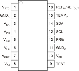
1.13 Pin Configuration
 Figure 1-2 PGA309 Pin Assignments
Table 1-2 PGA309 Pin Descriptions
| Pin | Name | Description |
|---|---|---|
| 1 | VEXC | Bridge sensor excitation. Connect to bridge if linearization and/or internal reference for bridge excitation is to be used. |
| 2 | GNDA | Analog ground. Connect to analog ground return path for VSA. Should be same as GNDD. |
| 3 | VSA | Analog voltage supply. Connect to analog voltage supply. To be within 200mV of VSD. |
| 4 | VIN1 | Signal input voltage 1. Connect to + or – output of sensor bridge. Internal multiplexer can change connection internally to Front-End PGA. |
| 5 | VIN2 | Signal input voltage 2. Connect to + or – output of sensor bridge. Internal multiplexer can change connection internally to Front-End PGA. |
| 6 | VFB | VOUT feedback pin. Voltage feedback sense point for over/under-scale limit circuitry. When internal gain set resistors for the Output Amplifier are used, this is also the
voltage feedback sense point for the Output Amplifier. VFB in combination with VSJ allows for ease of external filter and protection circuits without degrading the PGA309 VOUT accuracy. VFB must always be connected to either VOUT or the point of feedback for VOUT, if external protection is used. |
| 7 | VOUT | Analog output voltage of conditioned sensor. |
| 8 | VSJ | Output Amplifier summing junction. Use for Output Amplifier compensation when driving large capacitive loads (> 100pF) and/or for using external gain setting resistors for the Output Amplifier. |
| 9 | TEST | Test/External Controller Mode pin. Pull to GNDD in normal mode. |
| 10 | VSD | Digital voltage supply. Connect to digital voltage supply. To be within 200mV of VSA. |
| 11 | GNDD | Digital ground. Connect to digital ground return path for VSD. Should be same as GNDA. |
| 12 | PRG | Single-wire interface program pin. UART-type interface for digital calibration of the PGA309 over a single wire. Can be connected to VOUT for a three-lead (VS, GND, VOUT) digitally programmable sensor assembly. |
| 13 | SCL | Clock input/output for Two-Wire, industry-standard compatible interface for reading and writing digital calibration and configuration from external EEPROM. Can also communicate directly to the registers in the PGA309 through the Two-Wire, industry-standard compatible interface. |
| 14 | SDA | Data input/output for Two-Wire, industry-standard compatible interface for reading and writing digital calibration and configuration from external EEPROM. Can also communicate directly to the registers in the PGA309 through the Two-Wire, industry-standard compatible interface. |
| 15 | TEMPIN | External temperature signal input. PGA309 can be configured to read a bridge current sense resistor as an indicator of bridge temperature, or an external temperature sensing device such as diode junction, or RTD, or thermistor. This input can be internally gained up by 1, 2, 4, or 8. In addition, this input can be read differentially with respect to VGNDA, VEXC, or the internal VREF. There is also an internal, register-selectable, 7µA current source (ITEMP) that can be connected to TEMPIN as an RTD, thermistor, or diode excitation source. |
| 16 | REFIN/REFOUT | Reference input/output pin. As an output, the internal voltage reference (selectable as 2.5V or 4.096V) is avail-able for system use on this pin. As an input, the internal voltage reference may be disabled and an external voltage reference can then be applied as the reference for the PGA309. |