SBOU024C august 2004 – july 2023 PGA309
- 1
- Read This First
-
1Introduction
- 1.1 PGA309 Functional Description
- 1.2 Sensor Error Adjustment Range
- 1.3 Gain Scaling
- 1.4 Offset Adjustment
- 1.5 Voltage Reference
- 1.6 Sensor Excitation and Linearization
- 1.7 ADC for Temperature Sensing
- 1.8 External EEPROM and Temperature Coefficients
- 1.9 Fault Monitor
- 1.10 Over-Scale and Under-Scale Limits
- 1.11 Power-Up and Normal Operation
- 1.12 Digital Interface
- 1.13 Pin Configuration
- 2Detailed Description
- 3Operating Modes
-
4Digital Interface
- 4.1 Description
- 4.2 Two-Wire Interface
- 4.3 One-Wire Interface
- 4.4 One-Wire Interface Timeout
- 4.5 One-Wire Interface Timing Considerations
- 4.6 Two-Wire Access to External EEPROM
- 4.7 One-Wire Interface Initiated Two-Wire EEPROM Transactions
- 4.8 PGA309 Stand-Alone Mode and Two-Wire Transactions
- 4.9 PGA309 Two-Wire Bus Master Operation and Bus Sharing Considerations
- 4.10 One-Wire Operation with PRG Connected to VOUT
- 4.11 Four-Wire Modules and One-Wire Interface (PRG)
- 5Application Background
-
6Register Descriptions
- 6.1 Internal Register Overview
- 6.2
Internal Register Map
- 6.2.1 Register 0: Temp ADC Output Register (Read Only, Address Pointer = 00000)
- 6.2.2 Register 1: Fine Offset Adjust (Zero DAC) Register (Read/Write, Address Pointer = 00001)
- 6.2.3 Register 2: Fine Gain Adjust (Gain DAC) Register (Read/Write, Address Pointer = 00010)
- 6.2.4 Register 3: Reference Control and Linearization Register (Read/Write, Address Pointer = 00011)
- 6.2.5 Register 4: PGA Coarse Offset Adjust and Gain Select/Output Amplifier Gain Select Register (Read/Write, Address Pointer = 00100)
- 6.2.6 Register 5: PGA Configuration and Over/Under-Scale Limit Register (Read/Write, Address Pointer = 00101)
- 6.2.7 Register 6: Temp ADC Control Register (Read/Write, Address Pointer = 00110)
- 6.2.8 Register 7: Output Enable Counter Control Register (Read/Write, Address Pointer = 00111)
- 6.2.9 Register 8: Alarm Status Register (Read Only, Address Pointer = 01000)
- A External EEPROM Example
- B Detailed Block Diagram
- C Glossary
- Revision History
2.10 Noise and Coarse Offset Adjust
The PGA309 Front-End PGA contains auto-zero operational amplifiers that allow precision, low-noise measurements free from flicker, or 1/f noise, that is typically present in regular low-voltage CMOS op amps.
This auto-zero topology operates by canceling amplifier low-frequency noise and offset during each clock cycle of an internal oscillator. This flattens the low-frequency noise voltage spectrum of the PGA309, leaving only a small residual clock feedthrough component at ~7kHz and its multiples. Figure 2-27 details the PGA309 voltage noise spectrum for coarse offset adjust = 0mV. This auto-zero method allows higher precision measurement by filtering the output of the PGA309 proportionally. Conventional CMOS operational amplifiers that use averaging do not improve the signal-to-noise ratio in the 1/f noise region. In addition, the auto-zero technique allows the PGA309 input offset voltage to achieve very good temperature and time stability.
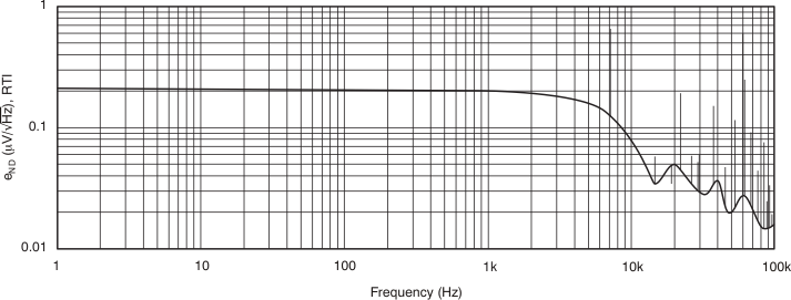 Figure 2-27 Voltage Noise Power Spectrum Referred to Input (RTI), Coarse Offset Adjust = 0mV, Gain = 1152, CLK_CFG = ‘00’ (default)
The PGA309 low-frequency voltage noise density (RTI) is ~210nV/√ Hz. To convert this to a peak-to-peak amplitude for oscilloscope measurements, the following equation is supplied:
VNPP = (eND)(√ BW)(crest factor)
where:
- VNPP = voltage noise peak-to-peak (nVPP)
- eND = voltage noise density (nV/√ Hz)
- BW = bandwidth of interest (Hz)
- Crest Factor = probability factor for conversion of rms noise to peak-to-peak noise (crest factor of 6 reduces probability of seeing a larger peak-to-peak amplitude to < 0.3%).
PGA309 peak-to-peak noise, RTI, BW = 10Hz:
VNPP = (210nV/√ Hz)(√10 Hz)(6) = 3984nVPP = 3.98μVPP (RTI)
For a PGA309 total gain of 1152, this implies the noise at VOUT will be 4.58mVPP , as shown in Figure 2-28.
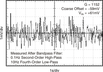 Figure 2-28 VOUT Noise, 0.1Hz to 10Hz Peak-to-Peak Noise
To compensate for bridge sensors with a large initial offset, the input stages of the PGA309 Front-End PGA incorporate a patented circuit for the coarse offset adjust based on the auto-zero topology. For each clock cycle of the internal auto-zero oscillator, the offsets and noise of the input amplifier stages are subtracted from the input signal, and the result is summed with a small voltage produced by the Coarse Offset Adjust DAC. This resulting value becomes the input-referred offset of the PGA309. This value can be positive or negative as described Section 2.2, Offset Scaling. This operation does not increase the low frequency 1/f noise of the PGA309. However, the mismatches of internal elements in the Coarse Offset DAC can produce temperature and long-term stability errors on the same order of magnitude as regular, traditional CMOS op amps (that is, temperature drift of input offset voltage of up to 10μV/°C).
To produce a value that is temperature- and time-stable, the Coarse Offset DAC circuitry incorporates a chopping circuit that rotates internal components, averaging the mismatch error on the output of the Coarse Offset Adjust DAC. This produces a very time- and temperature-stable coarse offset adjust.
The design compromise of the Coarse Offset DAC chopping technique is a clock feedthrough glitch that can be seen at VOUT, the output of the PGA309, due to the rotating elements. With the Coarse Offset Adjust set to 0mV the clock feedthrough components are practically negligible on the VOUT signal of the PGA309, as shown in Figure 2-29.
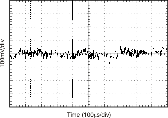 Figure 2-29 Unfiltered VOUT Clock Feedthrough, Coarse Offset Adjust = 0mV, Gain = 1152, CLK_CFG = ‘00’ (default)
As the Coarse Offset Adjust DAC value increases the amplitude of the clock, feedthrough glitch also increases. For VREF = +5V and a full-scale Coarse Offset DAC value of −59mV, the clock feedthrough glitch is shown in Figure 2-30. This scope photo is for the PGA309 set in its maximum internal gain of 1152, with the Coarse Offset Adjust DAC set to −59mV and VIN set to +61mV. Referred to input (RTI), this VOUT glitch is only 347μVPP (0.4VPP/1152). This glitch occurs at half of the internal auto-zero clock; typically, 3.5kHz. This glitch does not reflect back into the low-frequency range and can be filtered out if the signal of interest is at or below 1kHz. Figure 2-31 is a scope photo of VOUT peak-to-peak noise for this case. Figure 2-32 shows the voltage noise spectrum for the case where the Coarse Offset Adjust DAC is set to −59mV and VIN = +61mV. In Figure 2-32, the baseband noise is about the same as when the coarse offset adjust was set to zero, as in Figure 2-27, but with an additional spike at about 3.5kHz.
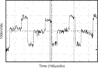 Figure 2-30 Unfiltered VOUT Clock Feedthrough Glitch, Coarse Offset Adjust = −59mV, Gain = 1152, VIN = +61mV, CLK_CFG = ‘00’ (default). VOUT Glitch (RTI) = 347µVPP
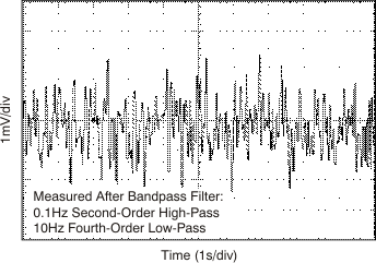 Figure 2-31 Filtered 0.1Hz to 10Hz VOUT Peak-to-Peak Noise, Coarse Offset Adjust = −59mV, Gain = 1152, VIN = +61mV, CLK_CFG = ‘00’ (default)
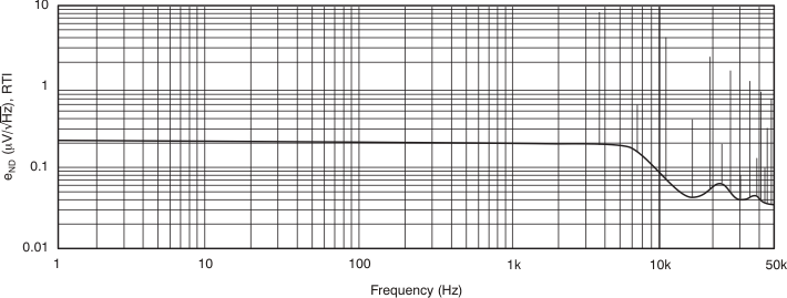 Figure 2-32 Voltage Noise Spectrum (RTI), Coarse Offset Adjust = −59mV, Gain = 1152, VIN = +61mV, CLK_CFG = ‘00’ (default)
For applications where the clock feedthrough glitch from the Coarse Offset Adjust DAC chopping circuitry is an issue, there are alternate modes that can be selected for the Coarse Offset DAC clocking and the auto-zero clocking of the Front-End PGA. Register 5 bits (13:12) are referenced as CLK_CFG1 and CLK_CFG0, respectively. Table 2-23 outlines the clocking schemes available using these bits. Up to this point, CLK_CFG = ‘00’ has been discussed.
| CLK_CFG Mode | CLK_CFG1 Bit D13 | CLK_CFG0 Bit D12 | Auto-Zero PGA Front-End | Chopping Coarse Offset DAC |
|---|---|---|---|---|
| 00 (default) | 0 | 0 | 7kHz typical | 3.5kHz typical |
| 01 | 0 | 1 | 7kHz typical | Off (none) |
| 10 | 1 | 0 | 7kHz typical, Random Clocking | 3.5kHz typical, Random Clocking |
| 11 | 1 | 1 | 7kHz typical | 3.5kHz typical, Random Clocking |
In the CLK_CFG = ‘01’ mode, the Coarse Offset Adjust DAC chopping is turned off. The clock feedthrough glitch is no longer present (Figure 2-33 shows the 0.1Hz to 10Hz VOUT peak-to-peak noise) and the VOUT noise spectrum is clean, as shown in Figure 2-34. However, the input Coarse Offset Adjust DAC is no longer temperature-stable. Typical span drift is generally linear with temperature and may be acceptable in applications where the PGA309 is located close to the bridge sensor and they are both calibrated together. The drift of the Coarse Offset Adjust DAC simply sums with the bridge sensor offset drift, and they are both calibrated out.
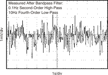 Figure 2-33 0.1Hz to 10Hz VOUT Peak-to-Peak Noise for Coarse Offset Adjust = −56mV, Gain = 1152, VIN = +57mV, CLK_CFG = ‘01’, VNPP (RTI) = 4.44 VPP
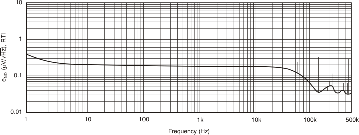 Figure 2-34 VOUT Noise Spectrum for Coarse Offset Adjust = −56mV, Gain = 1152, VIN = +57mV, CLK_CFG = ‘01’
CLK_CFG = ‘10’ mode and CLK_CFG = ‘11’ mode turn on different clock randomization schemes for the Front-End PGA auto-zero and Coarse Offset DAC chopping. Although this does not reduce the amplitude of the clock feedthrough glitch (see Figure 2-30), it does spread the glitch energy over a wider frequency range. This removes the fixed spike at half of the input auto-zero clock frequency, but raises the noise floor in the lower frequency range, thus increasing the baseband noise. CLK_CFG = ‘11’ mode simply whitens the peak-to-peak noise from the 1Hz region to about the 7kHz region by modulating both the auto-zero and chopping clocks. In CLK_CFG = ‘10’ mode, the Coarse Offset DAC chopping clock is modulated but not the auto-zero clock. The results of these two modes are shown in both voltage noise spectrum and peak-to-peak noise plots in Figure 2-35, Figure 2-36, Figure 2-37, and Figure 2-38.
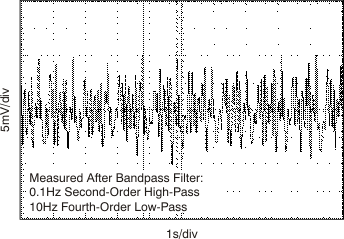 Figure 2-35 0.1Hz to 10Hz VOUT Peak-to-Peak Noise for Coarse Offset Adjust = −56mV, Gain = 1152, VIN = +57mV, CLK_CFG = ‘10’, VNPP (RTI) = 18.4µVPP
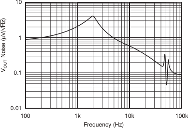 Figure 2-36 VOUT Noise Spectrum for Coarse Offset Adjust = −56mV, Gain = 1152, VIN = +57mV, CLK_CFG = ‘10’
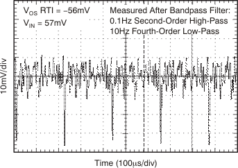 Figure 2-37 0.1Hz to 10Hz VOUT Peak-to-Peak Noise for Coarse Offset Adjust = −56mV, Gain = 1152, VIN = +57mV, CLK_CFG = ‘11’, VNPP (RTI) = 42µVPP
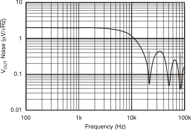 Figure 2-38 VOUT Noise Spectrum for Coarse Offset Adjust = −56mV, Gain = 1152, VIN = +57mV, CLK_CFG = ‘11’