SLAA654A November 2014 – July 2015 CC430F6147 , MSP430F412 , MSP430F413 , MSP430F4132 , MSP430F415 , MSP430F4152 , MSP430F417 , MSP430F423A , MSP430F4250 , MSP430F425A , MSP430F4260 , MSP430F4270 , MSP430F427A , MSP430F435 , MSP430F4351 , MSP430F436 , MSP430F4361 , MSP430F437 , MSP430F4371 , MSP430F438 , MSP430F439 , MSP430F447 , MSP430F448 , MSP430F4481 , MSP430F449 , MSP430F4491 , MSP430F4616 , MSP430F46161 , MSP430F4617 , MSP430F46171 , MSP430F4618 , MSP430F46181 , MSP430F4619 , MSP430F46191 , MSP430F47126 , MSP430F47127 , MSP430F47163 , MSP430F47166 , MSP430F47167 , MSP430F47173 , MSP430F47176 , MSP430F47177 , MSP430F47183 , MSP430F47186 , MSP430F47187 , MSP430F47193 , MSP430F47196 , MSP430F47197 , MSP430F477 , MSP430F478 , MSP430F4783 , MSP430F4784 , MSP430F479 , MSP430F4793 , MSP430F4794 , MSP430F6433 , MSP430F6435 , MSP430F6436 , MSP430F6438 , MSP430F6458 , MSP430F6459 , MSP430F6630 , MSP430F6631 , MSP430F6632 , MSP430F6633 , MSP430F6634 , MSP430F6635 , MSP430F6636 , MSP430F6637 , MSP430F6638 , MSP430F6658 , MSP430F6659 , MSP430F6720 , MSP430F6720A , MSP430F6721 , MSP430F6721A , MSP430F6723 , MSP430F6723A , MSP430F6724 , MSP430F6724A , MSP430F6725 , MSP430F6725A , MSP430F6726 , MSP430F6726A , MSP430F6730 , MSP430F6730A , MSP430F6731 , MSP430F6731A , MSP430F6733 , MSP430F6733A , MSP430F6734 , MSP430F6734A , MSP430F6735 , MSP430F6735A , MSP430F6736 , MSP430F6736A , MSP430F6745 , MSP430F67451 , MSP430F67451A , MSP430F6745A , MSP430F6746 , MSP430F67461 , MSP430F67461A , MSP430F6746A , MSP430F6747 , MSP430F67471 , MSP430F67471A , MSP430F6747A , MSP430F6748 , MSP430F67481 , MSP430F67481A , MSP430F6748A , MSP430F6749 , MSP430F67491 , MSP430F67491A , MSP430F6749A , MSP430F67621 , MSP430F67621A , MSP430F67641 , MSP430F67641A , MSP430F6765 , MSP430F67651 , MSP430F67651A , MSP430F6765A , MSP430F6766 , MSP430F67661 , MSP430F67661A , MSP430F6766A , MSP430F6767 , MSP430F67671 , MSP430F67671A , MSP430F6767A , MSP430F6768 , MSP430F67681 , MSP430F67681A , MSP430F6768A , MSP430F6769 , MSP430F67691 , MSP430F67691A , MSP430F6769A , MSP430F6775 , MSP430F67751 , MSP430F67751A , MSP430F6775A , MSP430F6776 , MSP430F67761 , MSP430F67761A , MSP430F6776A , MSP430F6777 , MSP430F67771 , MSP430F67771A , MSP430F6777A , MSP430F6778 , MSP430F67781 , MSP430F67781A , MSP430F6778A , MSP430F6779 , MSP430F67791 , MSP430F67791A , MSP430F6779A , MSP430FE423 , MSP430FE4232 , MSP430FE423A , MSP430FE4242 , MSP430FE425 , MSP430FE4252 , MSP430FE425A , MSP430FE427 , MSP430FE4272 , MSP430FE427A , MSP430FG4250 , MSP430FG4260 , MSP430FG4270 , MSP430FG437 , MSP430FG438 , MSP430FG439 , MSP430FG4616 , MSP430FG4617 , MSP430FG4618 , MSP430FG4619 , MSP430FG477 , MSP430FG478 , MSP430FG479 , MSP430FG6425 , MSP430FG6426 , MSP430FG6625 , MSP430FG6626 , MSP430FR4131 , MSP430FR4132 , MSP430FR4133 , MSP430FR5870 , MSP430FR5872 , MSP430FR58721 , MSP430FR5922 , MSP430FR59221 , MSP430FR5970 , MSP430FR5972 , MSP430FR59721 , MSP430FR6820 , MSP430FR6822 , MSP430FR68221 , MSP430FR6870 , MSP430FR6872 , MSP430FR68721 , MSP430FR6877 , MSP430FR6879 , MSP430FR68791 , MSP430FR6887 , MSP430FR6888 , MSP430FR6889 , MSP430FR68891 , MSP430FR6920 , MSP430FR6922 , MSP430FR69221 , MSP430FR6927 , MSP430FR69271 , MSP430FR6928 , MSP430FR6970 , MSP430FR6972 , MSP430FR69721 , MSP430FR6977 , MSP430FR6979 , MSP430FR69791 , MSP430FR6987 , MSP430FR6988 , MSP430FR6989 , MSP430FR69891 , MSP430FW423 , MSP430FW425 , MSP430FW427 , MSP430FW428 , MSP430FW429
- Designing With MSP430™ MCUs and Segment LCDs
- Revision History
4.2 Charge Pump
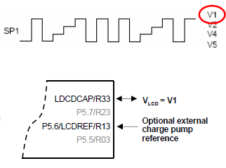
The VLCD voltage sets the voltage level of V1, the highest LCD voltage in the waveforms. This can be set in software to be sourced from AVCC, the internal charge pump, or from an external source. Most MSP430 LCD modules (LCD_A, LCD_B, LCD_C, and LCD_E) include a built-in charge pump – only the original LCD module on some F4xx devices does not have one.
The advantage of using a charge pump for generating the VLCD voltage is that: 1) it provides a regulated voltage to the LCD to keep a stable voltage output for the display, and 2) it allows you to have the VLCD set to a different voltage level that is independent of DVCC – this lets you set VLCD to the best level for the particular LCD display, and keep good contrast even as the battery in the system drains.
The built-in charge pump has programmable voltage levels for use with different segmented displays – the allowed maximum operating voltage is something that would come from the design of the particular LCD glass that is being used. Setting a different VLCD can change your contrast ratio, so having software-configurable voltage levels from the charge pump allows contrast control via software. For example, using a lower VLCD may provide less contrast, but also have less current consumption, so this is a trade-off to experiment with in a final design.
The charge pump requires an external capacitor for operation. If this capacitor is not present and the charge pump is turned on, the MSP430 device could be damaged. Because of this, some of the newer LCD modules like LCD_B and LCD_C include detection circuitry that automatically disable the charge pump if no capacitor is present, as well as setting an interrupt flag to warn user software of this condition. Note that the LCD_E module has a different configuration for the charge pump capacitor (connected between two pins instead of directly to ground), so it is not damaged if the capacitor is not present (though the charge pump does not work properly).
The charge pump can also be referenced to follow an external source. This is useful if multiple MSP430 MCUs are used together to control a single larger segmented display than could be controlled with a single device. The application note Use of Two MSP430 Microcontrollers to Enhance Segment Lines for Larger LCDs (SLAA072) describes how to do this.
 Figure 5. Charge Pump