SLOA277B january   2019  – july 2023 LM124 , LM124-N , LM124A , LM158 , LM158-N , LM158A , LM224 , LM224-N , LM224A , LM258 , LM258-N , LM258A , LM2902 , LM2902-N , LM2902-Q1 , LM2902K , LM2902KAV , LM2904 , LM2904-N , LM2904-Q1 , LM2904B , LM2904B-Q1 , LM2904BA , LM321 , LM324 , LM324-N , LM324A , LM358 , LM358-N , LM358A , LM358B , LM358BA , TS321 , TS321-Q1


  1.   1
  2.   Abstract
  3.   Trademarks
  4. 1Devices Covered in Application Note
    1. 1.1 Common Schematic
    2. 1.2 Base Part Numbers
    3. 1.3 Input Voltage Offset Grades
    4. 1.4 Maximum Supply Voltage
    5. 1.5 High Reliability Options
    6. 1.6 HBM ESD Grade
    7. 1.7 LM358B, LM358BA, LM2904B, LM2904BA, LM324B, LM2902B
  5. 2Input Stage Considerations
    1. 2.1 Input Stage Schematic
    2. 2.2 Input Common Mode Range
    3. 2.3 Input Impedance
    4. 2.4 Phase Reversal
  6. 3Output Stage Considerations
    1. 3.1 Output Stage Schematic, VOL and IOL
    2. 3.2 IOL and Common Mode Voltage
    3. 3.3 Output Stage Schematic, VOH and IOH
    4. 3.4 Short Circuit Sourcing Current
    5. 3.5 Output Voltage Limitations
  7. 4AC Performance
    1. 4.1 Slew Rate and Bandwidth
    2. 4.2 Slew Rate Variability
    3. 4.3 Output Crossover Time Delay
    4. 4.4 First Crossover Example
    5. 4.5 Second Crossover Example
  8. 5Low VCC Guidance
    1. 5.1 Low VCC Input Range Supporting –40°C
    2. 5.2 Low VCC Output Range Supporting –40°C
    3. 5.3 Low VCC Audio Amplifier Example
  9. 6Comparator Usage
    1. 6.1 Op Amp Limitations
    2. 6.2 Input and Output Voltage Ranges
    3. 6.3 Overload Recovery
    4. 6.4 Slew Rate
  10. 7Unused Amp Connections and Inputs Connected Directly to Ground
    1. 7.1 Do Not Connect Inputs Directly to Ground
    2. 7.2 Unused Amplifier Connections
  11. 8Conclusion
  12. 9Revision History

Input Stage Schematic

The input stage in Figure 2-1 contains additional current source lines (shown boxed in red) not drawn in the simplified schematic found in the data sheets. All PNP emitters in the Darlington input stage have current source connections. These connections ensure a consistent input bias current that does not vary with the differential input voltage. This consistent current provides a high effective input to input resistance. Without the red box current sources, the input bias current would vary from zero to twice the normal bias current as the differential input voltage is varied. This is common on other bipolar transistor input op amps. TS321 is an exception to this rule because it does not have the additional current sources.
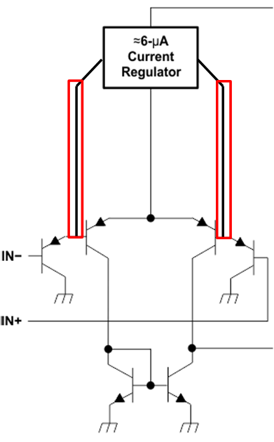
GUID-7122E16F-4A54-468A-9171-C7ACF4DE7620-low.gifFigure 2-1 Input Stage Schematic with All Current Source Connections