SLOA277B january 2019 – july 2023 LM124 , LM124-N , LM124A , LM158 , LM158-N , LM158A , LM224 , LM224-N , LM224A , LM258 , LM258-N , LM258A , LM2902 , LM2902-N , LM2902-Q1 , LM2902K , LM2902KAV , LM2904 , LM2904-N , LM2904-Q1 , LM2904B , LM2904B-Q1 , LM2904BA , LM321 , LM324 , LM324-N , LM324A , LM358 , LM358-N , LM358A , LM358B , LM358BA , TS321 , TS321-Q1
4.4 First Crossover Example
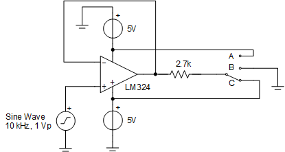
The first example test circuit in Figure 4-5 uses the LM324 as a 10-kHz frequency sine wave buffer. The input signal is a ±1-V peak, 10-kHz sine wave. The supply voltage is ±5 V. The load is always 2.7 kΩ, regardless of the switch position. But, the termination voltage for the resistor can be switched between –5 V, 0 V, and 5 V. Ideally, the op amp output would follow the input voltage sine wave as the load current is small and the output slew rate required is well below the typical slew rate specification.
 Figure 4-5 Crossover Test
Schematic
Figure 4-5 Crossover Test
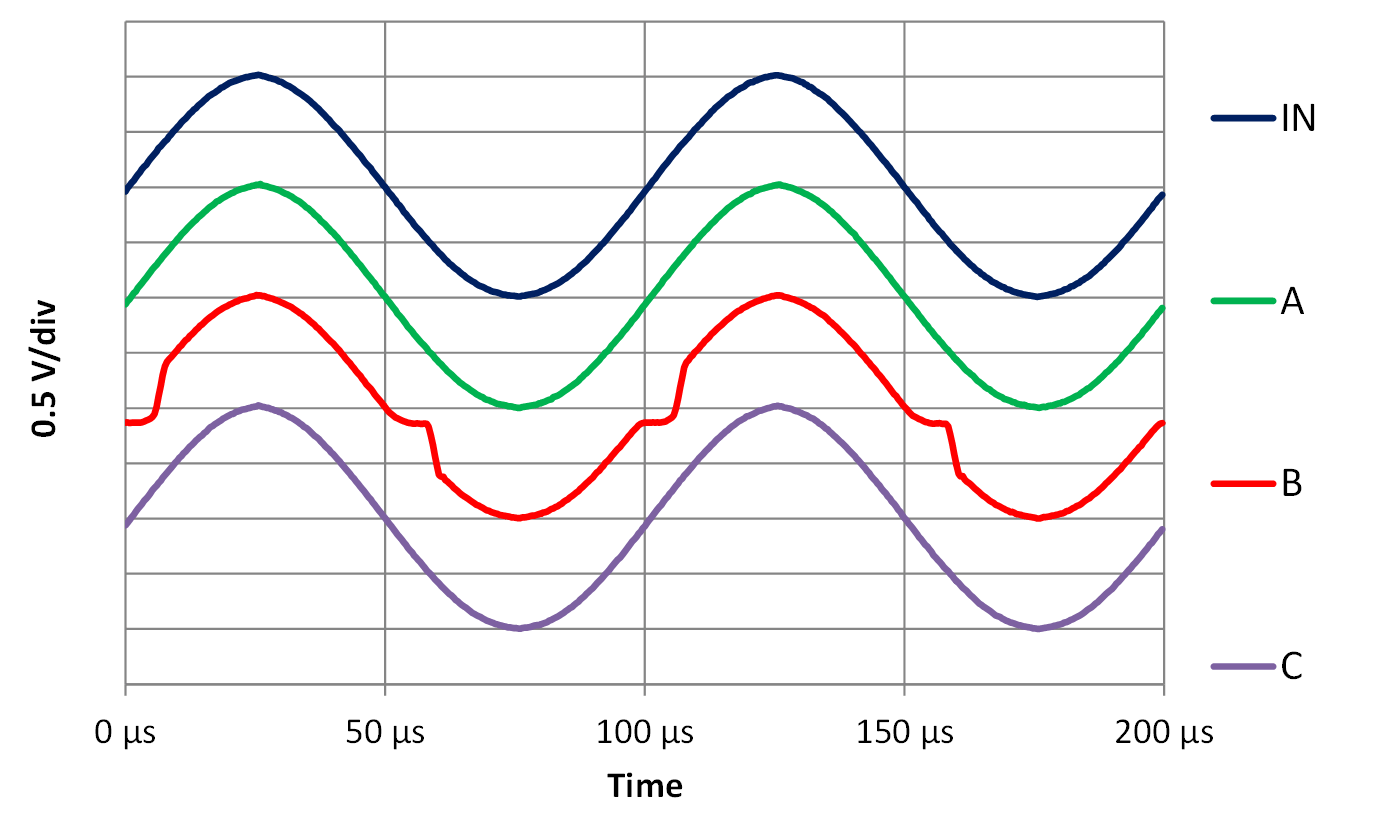
SchematicCase A: With the switch in position “A”, the load resistor is terminated to –5 V. So, the op amp will always source current. This current will vary from 1.48 mA to 2.22 mA. The output will follow the input as the Darlington NPN driver is always active as seen in the green waveform in Figure 4-6.
Case B: With the switch in position “B”, the load resistor is terminated to 0 V, or mid-supply. Therefore, the op amp will source and sink current, requiring the output to change drivers. The current will vary from –0.37 mA to 0.37 mA. Since the output driver will switch between PNP and NPN, the green box node voltage in Figure 4-4 has to slew to a voltage of three times VBE before the output voltage can change. At 25°C, the time needed to switch current polarity is
The output waveform flattens for 4 µs as only the weak constant current sink is active and neither the Darlington NPN driver nor the PNP emitter follower drivers are active during this time. See the red waveform in Figure 4-6. The voltage value of this flat time is 2.7 kΩ, or the load resistance, multiplied by the constant current sink value. After the delay, the output voltage changes at the device’s slew rate limit until it assumes the correct value. This happens each time the op amp switches between the source current and sink current drivers. The constant current sink is always on, but it is insufficient current to drive the 2.7-kΩ load resistor to –1 V by itself. Only the newest device simulation models dated 2018 or later include this time delay in the model.
Case C: With the switch in position “C”, the load resistor is terminated to 5 V. Thus, the op amp will always sink current. The current will vary from –1.48 mA to –2.22 mA. The output will follow the input as the PNP emitter follower will always be active. See the purple waveform in Figure 4-6.
 Figure 4-6 LM324 Crossover Test
Waveforms