SLUAAH0 February 2022 UCC14130-Q1 , UCC14131-Q1 , UCC14140-Q1 , UCC14141-Q1 , UCC14240-Q1 , UCC14241-Q1 , UCC14340-Q1 , UCC14341-Q1 , UCC15240-Q1 , UCC15241-Q1
- Trademarks
- 1 Introduction
- 2 Three-Phase Traction Inverter
- 3 Gate Drive Bias Requirements
- 4 Single Positive Isolated Output Voltage
- 5 Dual Positive and Negative Output Voltages
- 6 Dual Positive Output Voltages
- 7 Capacitor Selection
-
8 RLIM
Current Limit Resistor
- 8.1 RLIM Functional Description
- 8.2
RLIM
Dual Output Configuration
- 8.2.1 CVEE Above Nominal Value CVDD Below Nominal Value
- 8.2.2 CVEE Below Nominal Value CVDD Above Nominal Value
- 8.2.3 Gate Driver Quiescent Current: IQ_VEE > IQ_VDD
- 8.2.4 Gate Driver Quiescent Current: IQ_VEE < IQ_VDD
- 8.2.5 CVEE Above Nominal Value CVDD Below Nominal Value: IQ_VEE > IQ_VDD
- 8.2.6 CVEE Below Nominal Value CVDD Above Nominal Value: IQ_VEE < IQ_VDD
- 8.3 RLIM Single Output Configuration
- 9 UCC14240-Q1 Excel Design Calculator Tool
- 10Thermal Considerations
- 11Enable (ENA) and Power Good (/PG)
- 12PCB Layout Considerations
- 13Reference Design Example
- 14Summary
- 15References
10.3 Thermal Measurement and TJ Calculation Example
For the UCC14240-Q1 used in an EVM operating at VIN=24 V, VDD-VEE=20 V and POUT=1.62 W with η=57%, the power dissipation is determined as:
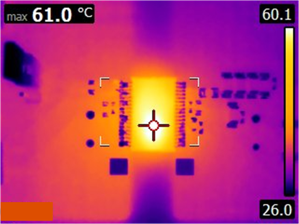
The maximum case temperature is measured as TC=61°C at TA=26°C ambient and the resulting thermal image is shown in Figure 10-1.

Figure 10-1 UCC14240-Q1 Max Case Temperature, POUT=1.62 W
Using the ΨJT thermal metric that was derived from the EVM closely representing how the UCC14240-Q1 PCB is expected to be designed, we obtain a TJ of 81.25°C as shown in Equation 41. Applying ΨJT is therefore considered the most accurate method for estimating TJ.
Compare to applying the RΘJC thermal resistance extracted from the JEDEC PCB which has less copper heat sink, no vias and thin copper traces extending from each IC pin, we obtain a TJ of 95.7°C as shown in Equation 42. The error in this result is mostly attributed to the PCB mismatch between the JEDEC PCB and the EVM as well as the thermal interface between the measured case temperature and die temperature.
Finally, applying the RΘJA thermal resistance, also extracted from the JEDEC PCB, which has less copper heat sink, no vias and copper fingers extending from each IC pin, we obtain a TJ of 89.8°C as shown in Equation 43. This result also assumes the error between the JEDEC PCB and the EVM but does not rely on measured case temperature and more closely agrees with Equation 43.