SLUAAH0 February 2022 UCC14130-Q1 , UCC14131-Q1 , UCC14140-Q1 , UCC14141-Q1 , UCC14240-Q1 , UCC14241-Q1 , UCC14340-Q1 , UCC14341-Q1 , UCC15240-Q1 , UCC15241-Q1
- Trademarks
- 1 Introduction
- 2 Three-Phase Traction Inverter
- 3 Gate Drive Bias Requirements
- 4 Single Positive Isolated Output Voltage
- 5 Dual Positive and Negative Output Voltages
- 6 Dual Positive Output Voltages
- 7 Capacitor Selection
-
8 RLIM
Current Limit Resistor
- 8.1 RLIM Functional Description
- 8.2
RLIM
Dual Output Configuration
- 8.2.1 CVEE Above Nominal Value CVDD Below Nominal Value
- 8.2.2 CVEE Below Nominal Value CVDD Above Nominal Value
- 8.2.3 Gate Driver Quiescent Current: IQ_VEE > IQ_VDD
- 8.2.4 Gate Driver Quiescent Current: IQ_VEE < IQ_VDD
- 8.2.5 CVEE Above Nominal Value CVDD Below Nominal Value: IQ_VEE > IQ_VDD
- 8.2.6 CVEE Below Nominal Value CVDD Above Nominal Value: IQ_VEE < IQ_VDD
- 8.3 RLIM Single Output Configuration
- 9 UCC14240-Q1 Excel Design Calculator Tool
- 10Thermal Considerations
- 11Enable (ENA) and Power Good (/PG)
- 12PCB Layout Considerations
- 13Reference Design Example
- 14Summary
- 15References
5 Dual Positive and Negative Output Voltages
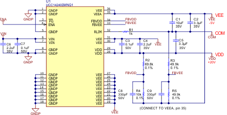
For optimal switching performance and robustness against dV/dt induced turn-on in half-bridge applications, many SiC MOSFETs and IGBTs benefit from a negative VEE voltage during turn-off. The UCC14240-Q1 greatly simplifies the task of establishing dual, positive and negative isolated output voltage rails when configured as shown in Figure 5-1.

Figure 5-1 Dual Positive, Negative Isolated Outputs
Similar to the single isolated output case of Figure 4-1, the total VDD-VEE is still set to +20 V as determined by the R2 and R4 divider with the midpoint connected to FBVDD (pin 34). However, the feedback pins, FBVDD (pin 34) and FBVEE (pin 33) are now separated and a second resistor divider, R3 and R5 is introduced with the midpoint connected to FBVEE (pin 33). R3 and R5 set the VEE regulation point anywhere within the range of 2.5 V<VEE<VDD-VEE. A capacitive divider between VDD and VEE establishes a virtual reference shown as COM at the midpoint. COM is the positive voltage reference with respect to VEE and the point where the VEE resistor divider is connected. The selection of the capacitive divider will be detailed in the Section 7 section. The FBVEE resistor divider is determined by selecting R5, then R3 can be calculated according to Equation 9.
Referencing the example circuit of Figure 5-1, the total regulated secondary-side voltage is VDD-VEE = +20 V, COM is desired to be +5 V with respect to VEE. Substituting COM = +5 V and VEE = 0 V (secondary-side reference point) into Equation 9 simplifies to R3=R5. For highest voltage setpoint accuracy, consider using 0.1% tolerance resistors, where the lower resistor, R5, shares the same reference point as the UCC14240-Q1 internal voltage reference at VEEA (U1-35). For a dual isolated output configuration, the introduction of the C1, C5 capacitive divider redefines the VDD reference point compared to the single output configuration. VDD in the dual output configuration is now given as VDD = +20 V-COM = +20 V-(+5 V) = +15 V and VEE= 0 V-COM = 0 V-(+5 V) = -5 V. The UCC14240-Q1, dual positive and negative voltage rails established for biasing any SiC/IGBT gate driver IC with respect to COM are now defined as: VDD = +15 V, and VEE = -5 V.
NOTE: When probing hardware, do not attach oscilloscope voltage probe ground leads to COM. Connecting probe ground to COM can result in a failed UCC14240-Q1 start-up, since COM is floating and the oscilloscope is referenced to earth ground. All oscilloscope voltage probe measurements made on the UCC14240-Q1 secondary should be referenced to VEE.