SLUAAH0 February 2022 UCC14130-Q1 , UCC14131-Q1 , UCC14140-Q1 , UCC14141-Q1 , UCC14240-Q1 , UCC14241-Q1 , UCC14340-Q1 , UCC14341-Q1 , UCC15240-Q1 , UCC15241-Q1
- Trademarks
- 1 Introduction
- 2 Three-Phase Traction Inverter
- 3 Gate Drive Bias Requirements
- 4 Single Positive Isolated Output Voltage
- 5 Dual Positive and Negative Output Voltages
- 6 Dual Positive Output Voltages
- 7 Capacitor Selection
-
8 RLIM
Current Limit Resistor
- 8.1 RLIM Functional Description
- 8.2
RLIM
Dual Output Configuration
- 8.2.1 CVEE Above Nominal Value CVDD Below Nominal Value
- 8.2.2 CVEE Below Nominal Value CVDD Above Nominal Value
- 8.2.3 Gate Driver Quiescent Current: IQ_VEE > IQ_VDD
- 8.2.4 Gate Driver Quiescent Current: IQ_VEE < IQ_VDD
- 8.2.5 CVEE Above Nominal Value CVDD Below Nominal Value: IQ_VEE > IQ_VDD
- 8.2.6 CVEE Below Nominal Value CVDD Above Nominal Value: IQ_VEE < IQ_VDD
- 8.3 RLIM Single Output Configuration
- 9 UCC14240-Q1 Excel Design Calculator Tool
- 10Thermal Considerations
- 11Enable (ENA) and Power Good (/PG)
- 12PCB Layout Considerations
- 13Reference Design Example
- 14Summary
- 15References
7 Capacitor Selection
The UCC14240-Q1 input and output high-frequency decoupling capacitors should consist of a 2.2-µF ceramic capacitor in parallel with a 0.1-µF ceramic capacitor as shown in Figure 7-1 and Figure 7-2. The 0.1-µF capacitor should be placed closest to the IC pins and both capacitors should be rated for at least 1.5 times the applied voltage or a minimum voltage rating of 35 V. The UCC14240-Q1 feedback resistor dividers require a 330-pF ceramic, high-frequency, bypass capacitor in parallel with the lower resistor. The 330-pF bypass capacitors are shown in the schematics of Figure 4-1 through Figure 6-1 and should be placed as close as possible between FBVDD (U1-34) and VEEA (U1-35) and FBVEE (U1-33) and VEEA (U1-35).
Figure 7-1 Turn-on Current Source
The circuits shown in Figure 7-1 and Figure 7-2 are illustrating source and sink current flow during turn-on and turn-off of an IGBT. The UCC14240-Q1 is providing dual positive and negative bias voltage to the UCC21732-Q1, ±10 A isolated, SiC/IGBT gate driver, driving an IGBT with 1.75 µC total gate charge. The diagrams have been simplified to highlight the functionality and selection of CVDD and CVEE. CVDD and CVEE are capacitors associated with the gate driver but also have a profound impact on the UCC14240-Q1 performance when using the dual, VDD/VEE output voltage configuration shown in Figure 5-1.
CVDD is the UCC21732-Q1, VDD bulk capacitor supplying the required charge to Q1 during turn-on and should be placed as close as possible to the gate driver pins. The total charge removed from CVDD by ISRC must be replenished by IDD every switching cycle. The removal and replenishing of charge into CVDD occur at the rate of the switching frequency of the IGBT and results in an unavoidable ripple voltage variation across CVDD. Since the total charge is supplied by the series combination of CVDD and CVEE, assuming a desired ripple voltage limit of ΔV=500 mVPP, the total required capacitance can be determined by Equation 10, where lower ripple voltage can be achieved at the cost of higher capacitance.
The equivalent capacitance, CG, required according to the IGBT gate charge of 1.75 µC is significantly less compared to the capacitance required by Equation 11. Therefore, the capacitance required to maintain a desired ripple voltage will always dominate over the CG required by a SiC/IGBT, as verified by 3.5 µF>>87.5 nF.
During turn-on, the IGBT requires an amount of power from CVDD which results in an equivalent amount of power delivered from the UCC14240-Q1 and is given by Equation 12 as:
During turn-off, the total charge stored in the IGBT gate capacitance is removed by applying CVEE (-5 V) in parallel with the IGBT, VGE. The power removed from CVEE during turn-off must also be replenished and delivered from the UCC14240-Q1 and is given by Equation 13 as:
The total dynamic power required, due to switching, is the sum of Equation 12 and Equation 13:
From the UCC21732-Q1 data sheet, the maximum IQ_VDD of 5.9-mA is used to calculate the power required due to quiescent current as:
Combining PSW and PIQ gives the total required bias power according to Equation 16:
The result of Equation 16 should be used to verify the required power is less than the maximum UCC14240-Q1 power of 1.5 W up to 105°C ambient temperature. For this example, the result is 847.5 mW<1.5 W.
Figure 7-2 Turn-off Current Sink
Equation 10 can be rewritten as:
A second function of the CVDD, CVEE capacitive divider is to balance the midpoint COM voltage according to the desired value of negative VEE voltage relative to positive VDD voltage. The voltage divider formed by CVDD and CVEE results in:
Setting Equation 17 equal to Equation 18 and solving for CVDD gives:
CVDD=4.67 µF which can then be used to solve for CVEE in Equation 20.
It is worth repeating that CVDD and CVEE are the minimum total capacitance values required by VDD and VEE with respect to COM. Add appropriate de-rating and choose standard component values greater than the calculated minimum results shown, then adjust to maintain the correct CVDD to CVEE ratio according to Equation 20. Once the values are chosen, CVDD and CVEE can now be substituted into Equation 10 and Equation 19 to verify the selected capacitor values meet the desired ΔV, ripple voltage as well as setting the correct midpoint voltage established by Equation 19. It might be necessary to use parallel combinations of different capacitor component values to obtain the desired ratio.
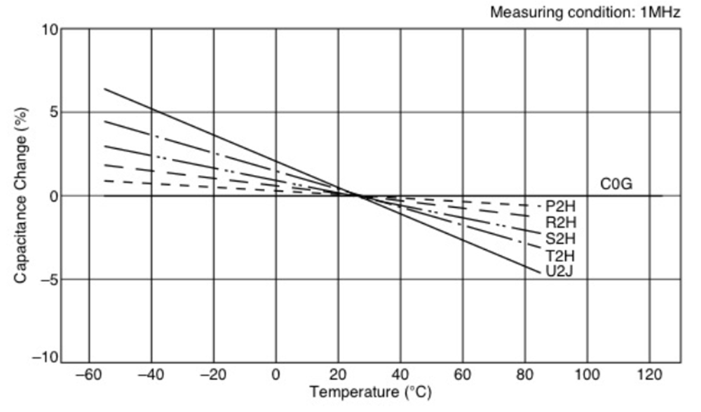
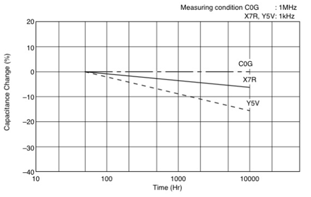
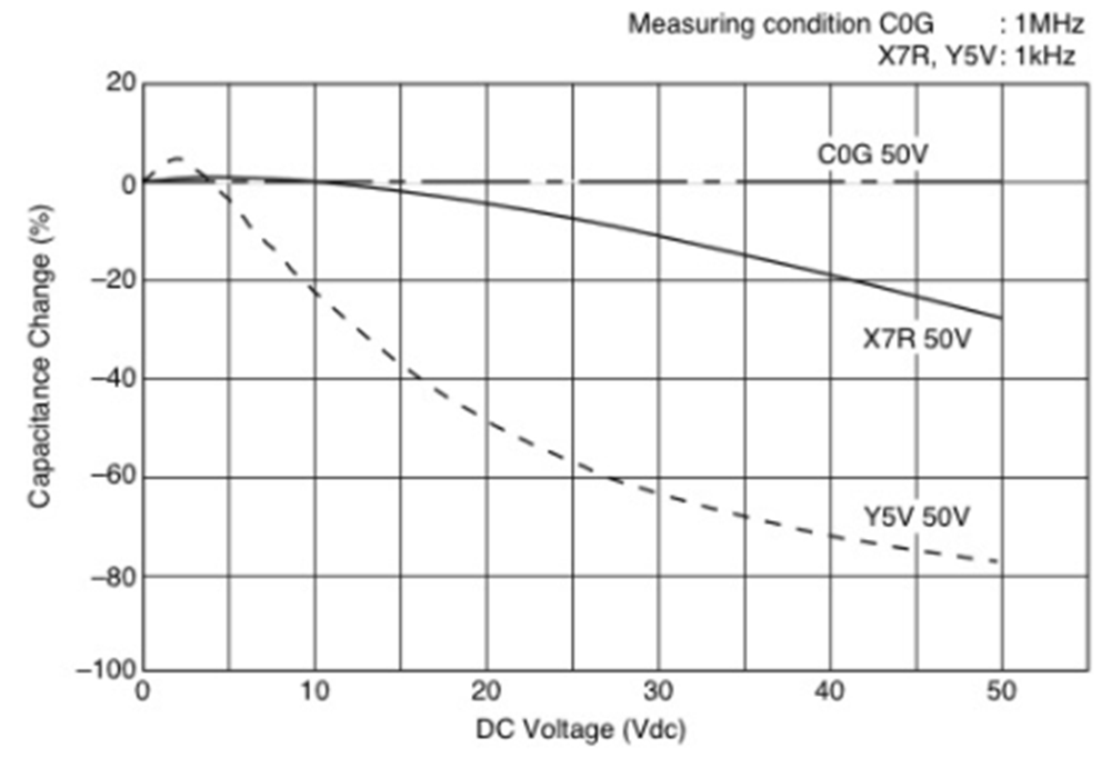
Reducing ripple voltage, VCE droop voltage or improving dynamic gate drive performance are a few possible reasons for increasing CVDD capacitor values. In an effort to maintain the correct CVDD to CVEE capacitor divider ratio (3:1 in this example), it important to scale the value of the CVEE capacitors to match any changes introduced to the CVDD capacitor value. CVDD capacitors should be 35-V or higher but CVEE capacitors can be rated at lower voltage, appropriately de-rated to handle ~1.5x VEE. CVDD and CVEE capacitors should be surface mount, ceramic X7R or better dielectric, AEC-Q200 rated for the intended temperature demands of the application. When trying to achieve the minimum required capacitance, careful attention should be paid to the applied DC voltage vs capacitor rated working voltage, temperature, tolerance and dielectric type as shown in Figure 7-3 through Figure 7-5. Achieving optimal bias and gate driver performance requires that minimum calculated capacitance is met under all electrical and environmental operating conditions.

Figure 7-3 Ceramic Capacitor Temperature Characteristics

Figure 7-4 Ceramic Capacitor Aging Characteristics

Figure 7-5 Ceramic Capacitor Applied DC Voltage Characteristics