SLUAAH0 February 2022 UCC14130-Q1 , UCC14131-Q1 , UCC14140-Q1 , UCC14141-Q1 , UCC14240-Q1 , UCC14241-Q1 , UCC14340-Q1 , UCC14341-Q1 , UCC15240-Q1 , UCC15241-Q1
- Trademarks
- 1 Introduction
- 2 Three-Phase Traction Inverter
- 3 Gate Drive Bias Requirements
- 4 Single Positive Isolated Output Voltage
- 5 Dual Positive and Negative Output Voltages
- 6 Dual Positive Output Voltages
- 7 Capacitor Selection
-
8 RLIM
Current Limit Resistor
- 8.1 RLIM Functional Description
- 8.2
RLIM
Dual Output Configuration
- 8.2.1 CVEE Above Nominal Value CVDD Below Nominal Value
- 8.2.2 CVEE Below Nominal Value CVDD Above Nominal Value
- 8.2.3 Gate Driver Quiescent Current: IQ_VEE > IQ_VDD
- 8.2.4 Gate Driver Quiescent Current: IQ_VEE < IQ_VDD
- 8.2.5 CVEE Above Nominal Value CVDD Below Nominal Value: IQ_VEE > IQ_VDD
- 8.2.6 CVEE Below Nominal Value CVDD Above Nominal Value: IQ_VEE < IQ_VDD
- 8.3 RLIM Single Output Configuration
- 9 UCC14240-Q1 Excel Design Calculator Tool
- 10Thermal Considerations
- 11Enable (ENA) and Power Good (/PG)
- 12PCB Layout Considerations
- 13Reference Design Example
- 14Summary
- 15References
4 Single Positive Isolated Output Voltage
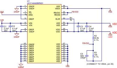
For SiC MOSFETs or IGBTs requiring only a single isolated output voltage, the UC14240-Q1 can be configured to regulate between 18 V<VDD-VEE<25 V. Connecting pin 33 to pin 34 allows a single feedback resistor divider, R2, R3 connected between VDD and VEE to set the regulation voltage as shown in Figure 4-1. The feedback pin serves as the inverting input to a hysteretic comparator. The non-inverting input is a precision, trimmed 2.5-V source, internally referenced to VEEA. For highest voltage set point accuracy, consider using 0.1% tolerance resistors, where the lower resistor, R3, shares the same reference point as the internal voltage reference at VEEA (U1-35). By selecting R3, then R2 can be calculated according to Equation 8.
The circuit shown in Figure 4-1 is an example showing VDD = +20 V with respect to VEE. VEE can be referenced to any secondary-side, low-side ground or the switch-node, midpoint of a half-bridge configuration for high-side bias needs.

Figure 4-1 Single Isolated Output