SLUP412 February 2022 LMG3522R030-Q1
- 1 Introduction
- 2 Comparing Different Technologies
- 3 Advantages of Integrating the Driver With GaN FETs
- 4 The GaN-Based 6.6-kW OBC Reference Design
- 5 PFC Stage
- 6 DC/DC Stage
- 7 DC/DC Topology Selection
- 8 Frequency Selection
- 9 Core Loss
- 10Loss of ZVS
- 11Dead Time
- 12ISR Bandwidth
- 13Overall
- 14Resonant Tank Design
- 15Thermal Solution
- 16Layout Best Practices
- 17Control-Loop Considerations
- 18Conclusions
- 19References
- 20Important Notice
5 PFC Stage
To reach a power density target of more than 60 W/inch3, it’s important to design the PFC with the smallest possible number of components while still maintaining good efficiency and keeping the components within their thermal limits. With these requirements, the topology of choice is the totem-pole bridgeless PFC [10][11].
After having selected the PFC topology, the next step in the design process is to decide on a mode of operation: CCM or critical conduction mode (CrCM). For both modes of operation, Figure 5-1 illustrates the envelope of the actual current waveform and the average current waveform for a single AC half cycle.
The average current is identical for both modes, but by leveraging different inductance values and control schemes, the shape of the actual current waveform is completely different.
CCM operation offers a smaller inductor current ripple and thus smaller root-mean-square (RMS) current stress in the FETs. CrCM operation enables zero-voltage switching of the FETs when the input voltage is smaller than half the output voltage. For higher input voltages, it is possible to turnon the FETs with a reduced voltage, because the current always returns to 0 A before every new switching cycle.
With CCM operation, the power stage is hard switching, which means that the FETs will exhibit losses at every turnon and turnoff transition. Thus, CCM produces higher switching losses in the FETs than CrCM operation.
Large reverse-recovery charge losses would prevent the use of CCM operation with silicon FETs. In CrCM, there are no reverse-recovery losses because the current always returns to 0 A. Given the zero reverse-recovery charge characteristic of directly driven TI GaN FETs, these losses are also out of the equation for CCM operation and make it an attractive alternative.
Choosing an inductance value for CrCM operation that’s several times smaller than in CCM has the potential to reduce inductor size. The peak and RMS currents in the FETs will be several times larger than in CCM, however.
For the 6.6-kW OBC reference design and its 30-mΩ TI GaN FETs, the larger RMS currents would have required the use of a three-phase CrCM PFC approach in order to keep all components within their thermal limits. In CCM, with a two-phase approach, the GaN FETs would stay within their thermal limits.
A multiphase approach distributes the losses among more components and spreads them to a wider area. In addition, these components may have slightly more disadvantageous parameters, such as higher direct current resistance (DCR) and lower Isat for inductors, or higher RDS(on) for the FETs than in a single-phase configuration. Thus, leveraging a multiphase converter makes it easier to find more cost-effective and fitting components for a high-power design.
Figure 5-2 shows the relative loss reduction for one-, two- and three-phase 6.6-kW CCM PFC switching at 120 kHz. The loss reduction from one to two phases is roughly 40%. Adding a third phase makes sense if the main design target is to maximize efficiency.
Three factors determine the choice of operating switching frequency: the power density target, the efficiency and the electromagnetic interference (EMI) limit lines. There will have to be a trade-off between raising the switching frequency to improve the power density and reducing the switching frequency to optimize converter efficiency.
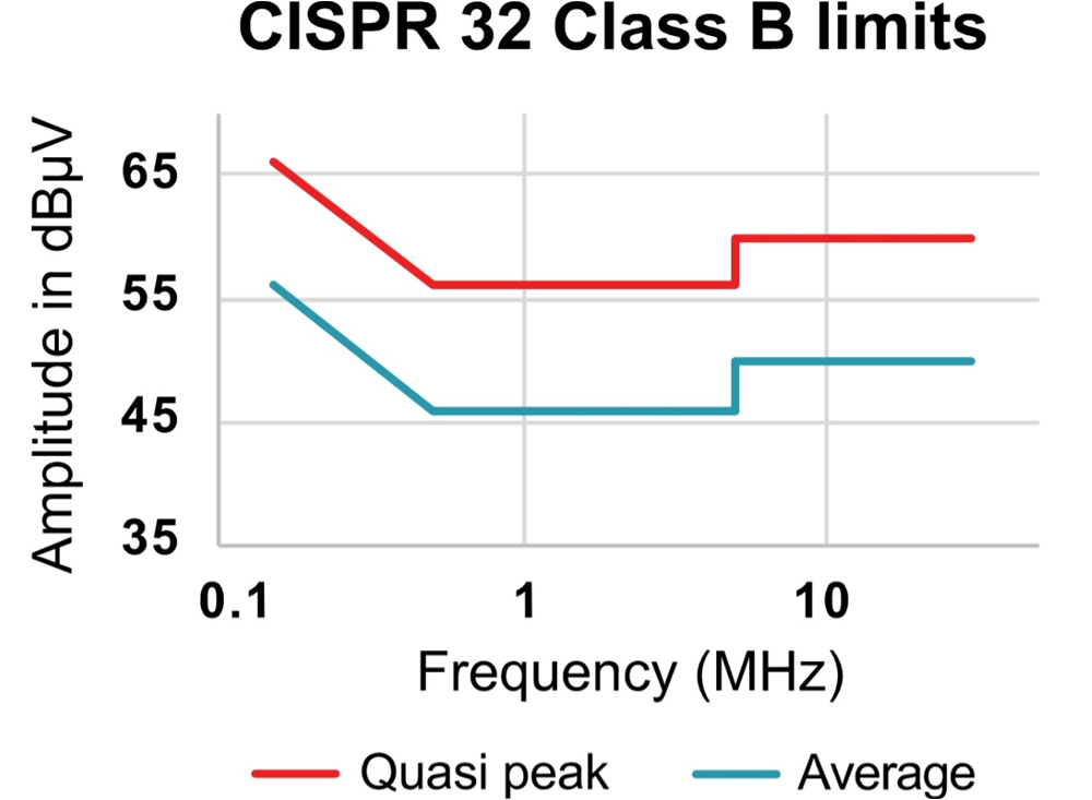
It is also important to remember the worst-case limit lines of the EMI standard against those you need to test the design to test the design. For multiphase converters, consider the effective switching frequency for the electromagnetic measurement, which is n-times the base switching frequency of each phase, where n is the number of phases. You also need to consider that the switching frequency for a PFC converter operating in CrCM is variable, which requires a more complex EMI filter design. Figure 5-3 shows the limit lines for CISPR 32 Class B.
 Figure 5-3 CISPR 32 Class B
limits.
Figure 5-3 CISPR 32 Class B
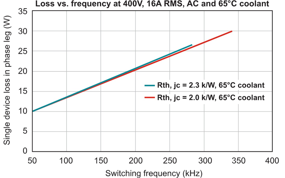
limits.A switching frequency of 120 kHz was chosen for this design, as the losses per GaN device would still keep them comfortably below the recommended maximum junction temperature, while the power dissipation is in a range that enables PFC efficiency of more than 98%.
Figure 5-4 illustrates the TI GaN FET losses over switching frequency for two different thermal resistances. The end of each graph indicates where the device reaches its maximum acceptable junction temperature.
 Figure 5-4 Single GaN device losses vs.
switching frequency for different thermal resistances to the thermal
interface.
Figure 5-4 Single GaN device losses vs.
switching frequency for different thermal resistances to the thermal
interface.Using a negatively coupled inductor instead of two separate PFC inductors will further improve the power density of an interleaved dual-phase totem-pole PFC converter. Negative coupling means that the orientation of the coupled winding ends is inverted (as shown in Figure 4-1), where the coupling dots are located at opposite sides.
The resulting ripple-current cancellation in this negatively coupled configuration can significantly lower the required inductance for each leg compared to a single inductor, while having a similar output ripple level. And, also introduces the option to use a slightly smaller core. For this design, the volume reduction was around 30% compared to a two-phase PFC implementation using two separate inductors.
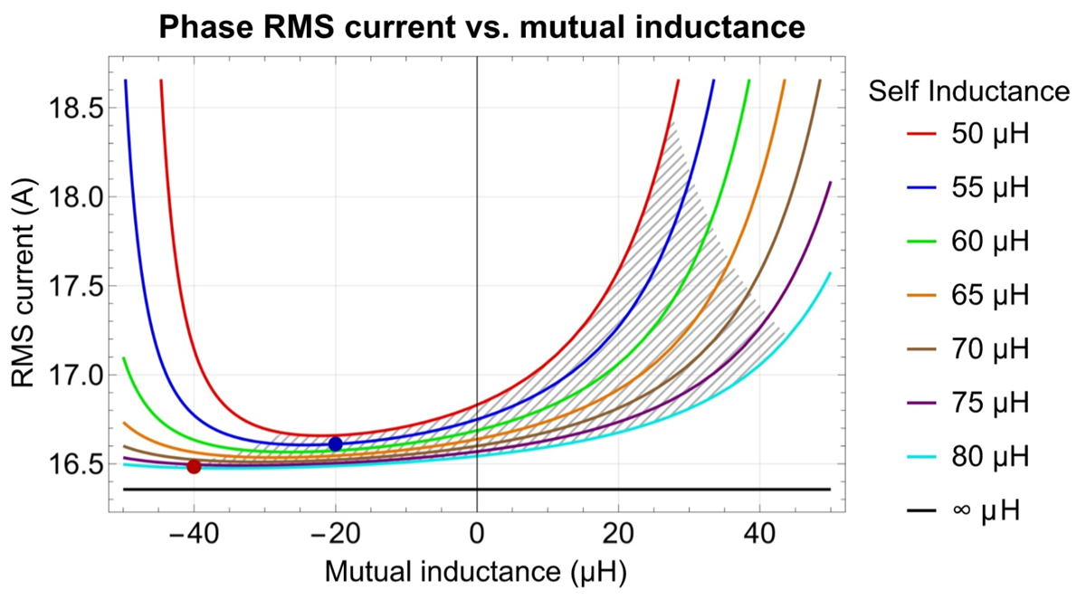
Figure 5-5 shows the effect of the coupling coefficient on the RMS current per phase for different self-inductance values.
 Figure 5-5 Single-phase RMS current vs.
mutual inductance: the grayed-out area is not manufacturable, the blue dot
indicates the optimal combination, and the red dot represents the coupled
inductor used in the 6.6-kW OBC reference design.
Figure 5-5 Single-phase RMS current vs.
mutual inductance: the grayed-out area is not manufacturable, the blue dot
indicates the optimal combination, and the red dot represents the coupled
inductor used in the 6.6-kW OBC reference design.Choosing the correct values for the self- and mutual inductance of this coupled inductor is a bit tricky, because the optimal simulated results are mechanically not manufacturable, as indicated by the grayed-out area in Figure 5-5. Only by having a “bad” coupling coefficient can you achieve the optimal ripple-current cancellation. The worse coupling also reduces the common-mode noise generated by the coupled inductor.
When using an interleaved approach, two phases with a 180-degree phase shift and negative coupling yield better ripple-current cancellation than positive coupling. The coupled inductor used in the 6.6-kW OBC reference design leverages two stacked 0079439A7 Kool Mµ® Max 60-µ cores with 77 µH of self-inductance, a coupling coefficient of 55% and a DCR of 12 mΩ per winding.
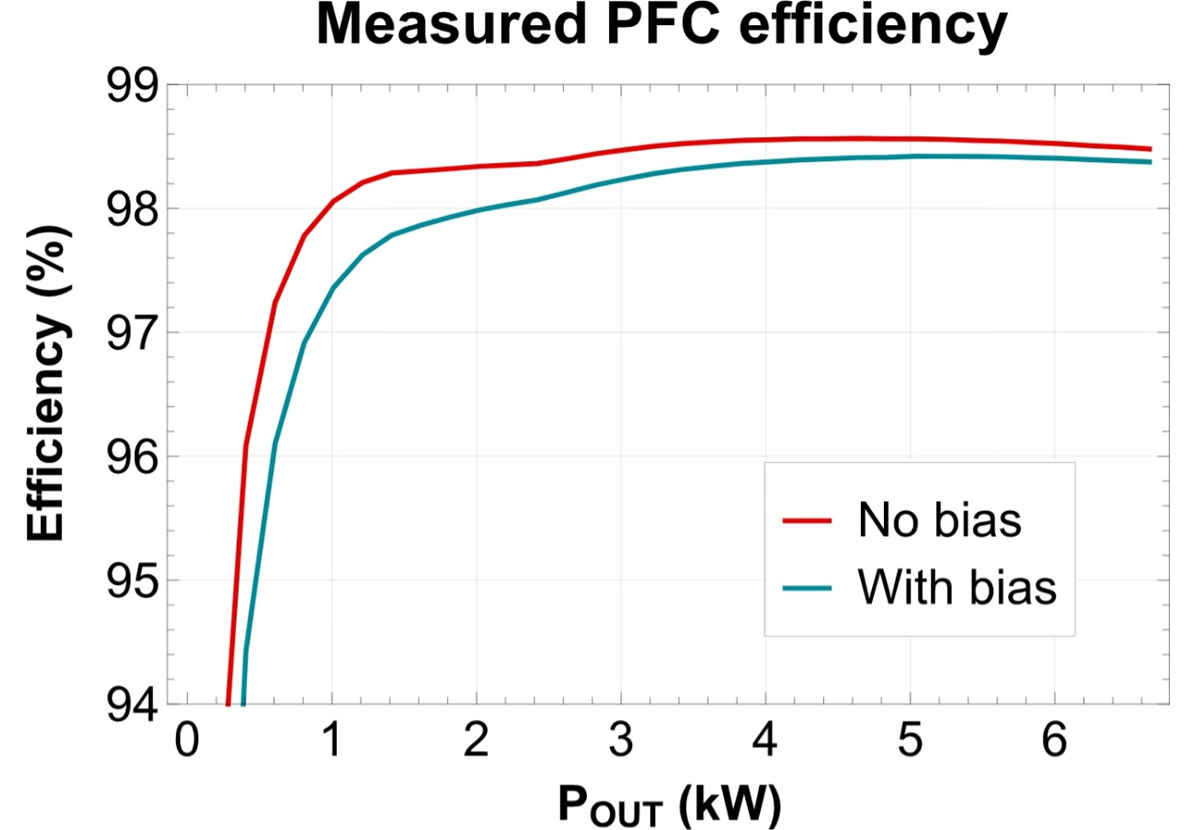
Measured efficiency data for the PFC (Figure 5-6) shows that it is possible to reach more than 98% efficiency at 30% output power and above, leveraging 650-V 30-mΩ GaN FETs in a very compact form factor.
 Figure 5-6 Measured efficiency of the PFC
converter accounting for the bias supplies (in blue) and not accounting for the
bias supplies (in red).