SPRACN0F October 2021 – March 2023 F29H850TU , F29H859TU-Q1 , TMS320F280021 , TMS320F280021-Q1 , TMS320F280023 , TMS320F280023-Q1 , TMS320F280023C , TMS320F280025 , TMS320F280025-Q1 , TMS320F280025C , TMS320F280025C-Q1 , TMS320F280033 , TMS320F280034 , TMS320F280034-Q1 , TMS320F280036-Q1 , TMS320F280036C-Q1 , TMS320F280037 , TMS320F280037-Q1 , TMS320F280037C , TMS320F280037C-Q1 , TMS320F280038-Q1 , TMS320F280038C-Q1 , TMS320F280039 , TMS320F280039-Q1 , TMS320F280039C , TMS320F280039C-Q1 , TMS320F280040-Q1 , TMS320F280040C-Q1 , TMS320F280041 , TMS320F280041-Q1 , TMS320F280041C , TMS320F280041C-Q1 , TMS320F280045 , TMS320F280048-Q1 , TMS320F280048C-Q1 , TMS320F280049 , TMS320F280049-Q1 , TMS320F280049C , TMS320F280049C-Q1 , TMS320F28374D , TMS320F28374S , TMS320F28375D , TMS320F28375S , TMS320F28375S-Q1 , TMS320F28376D , TMS320F28376S , TMS320F28377S , TMS320F28377S-Q1 , TMS320F28378D , TMS320F28378S , TMS320F28379D , TMS320F28379D-Q1 , TMS320F28379S , TMS320F28384D , TMS320F28384S , TMS320F28386D , TMS320F28386S , TMS320F28388D , TMS320F28388S , TMS320F28P650DH , TMS320F28P650DK , TMS320F28P650SH , TMS320F28P650SK , TMS320F28P659DH-Q1 , TMS320F28P659DK-Q1 , TMS320F28P659SH-Q1
- The Essential Guide for Developing With C2000™ Real-Time Microcontrollers
- Trademarks
- 1C2000 and Real-Time Control
-
2Sensing Key Technologies
- 2.1 Accurate Digital Domain Representation of Analog Signals
- 2.2 Optimizing Acquisition Time vs Circuit Complexity for Analog Inputs
- 2.3 Hardware Based Monitoring of Dual-Thresholds Using a Single Pin Reference
- 2.4 Resolving Tolerance and Aging Effects During ADC Sampling
- 2.5 Realizing Rotary Sensing Solutions Using C2000 Configurable Logic Block
- 2.6 Smart Sensing Across An Isolation Boundary
- 2.7 Enabling Intra-Period Updates in High Bandwidth Control Topologies
- 2.8 Accurate Monitoring of Real-Time Control System Events Without the Need for Signal Conditioning
-
3Processing Key Technologies
- 3.1 Accelerated Trigonometric Math Functions
- 3.2 Fast Onboard Integer Division
- 3.3 Hardware Support for Double-Precision Floating-Point Operations
- 3.4 Increasing Control Loop Bandwidth With An Independent Processing Unit
- 3.5 Flexible System Interconnect: C2000 X-Bar
- 3.6 Improving Control Performance With Nonlinear PID Control
- 3.7 Understanding Flash Memory Performance In Real-Time Control Applications
- 3.8 Deterministic Program Execution With the C28x DSP Core
- 3.9 Efficient Live Firmware Updates (LFU) and Firmware Over-The-Air (FOTA) updates
-
4Control Key Technologies
- 4.1 Reducing Limit Cycling in Control Systems With C2000 HRPWMs
- 4.2 Shoot Through Prevention for Current Control Topologies With Configurable Deadband
- 4.3 On-Chip Hardware Customization Using the C2000 Configurable Logic Block
- 4.4 Fast Detection of Over and Under Currents and Voltages
- 4.5 Improving System Power Density With High Resolution Phase Control
- 4.6 Safe and Optimized PWM Updates in High-Frequency, Multi-Phase and Variable Frequency Topologies
- 4.7 Solving Event Synchronization Across Multiple Controllers in Decentralized Control Systems
- 5Interface Key Technologies
- 6Safety Key Technologies
- 7References
- 8Revision History
5.3.2 In Depth
There are a number of serial communication peripherals to choose from when designing a multi-device real-time control system. With processors needing to pass critical data between each other within very short periods of time, latency is a primary concern for the system designer.
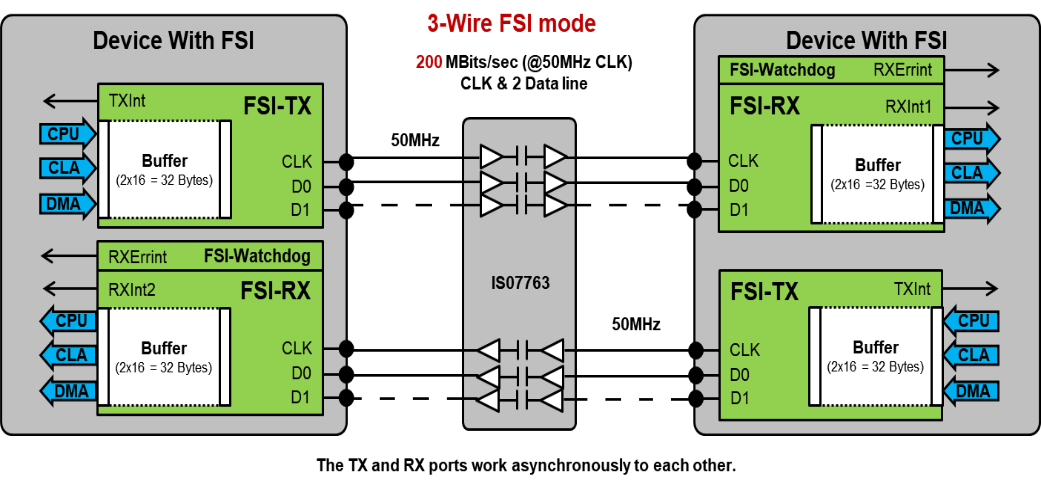
 Figure 5-4 Full Duplex 3-Wire FSI
Implementation
Figure 5-4 Full Duplex 3-Wire FSI
ImplementationSingle data (D0) and clock (CLK) is minimum set of signals for FSI communications at 100Mbps with lowest signal count and isolation cost. #T5843526-290 shows that signal D1 is an optional data line used to achieve the full 200Mbps data rate of the FSI.
The FSI physical interface consists of three wires, a clock and two data signals, where one of the data signals is optional (see #T5843526-290). Data is transferred on both the rising and falling edge which permits a 50 MHz maximum FSI clock frequency to transfer data at 100 Mbps with two wires (CLK and D0) and 200 Mbps with three wires (CLK, D0, and D1). The high through-put along with defined data packets (frames) that contain limited header and footer allows data to be transferred between devices with very little latency. The FSI module consists of independent transmitter and receiver cores which allow for simultaneous full speed communications in both directions with no concept of a master or slave. A real-time system using FSI for distributed control is showcased in Distributed Multi-axis Servo Drive Over Fast Serial Interface (FSI) Reference Design.
Features that FSI offers over other commonly used communications peripherals include:
- Hardware implemented CRC at both the transmitter and receiver side eliminating the CPU overhead of a SW implementation
- Delay line control at the receiver module to compensate for channel-to-channel skew
- Line break detection using ping and data frame watchdogs
- FSI protocol has no concept of masters and slaves enabling devices to send feedback at any time without the master device having to make a request
- High bit rate with low signal count reduces the amount of isolators needed in the system
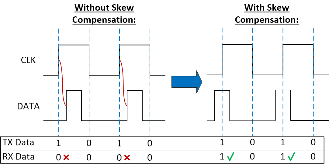
There are a number of system topologies which have components operating on both the “hot” (high voltage) and “cold” (low voltage) sides of the system that must communicate with each other. In this case digital isolators are used to bring data across an isolation barrier and the potential skew between signals that cross the isolation boundary can prove difficult to predict across many units of production. Even in systems without isolation, skew could be introduced by unequal signal trace lengths.
The delay line control feature at the receiver makes FSI well suited for this application as it can actively compensate for this skew (#T5843526-289) by adding delay to the individual FSI signals. See the Fast Serial Interface (FSI) Skew Compensation for more information on this differentiated feature. Also see the TMDSFSIADAPEVM for hardware evaluation of FSI with digital isolators.
 Figure 5-5 FSI Skew Compensation
Data is always transmitted and received on both the rising and falling edges of the FSI clock.
While only one data line is show in #T5843526-289 there is option of second data line in all FSI implementations