TIDT293 October   2022


  1.   Description
  2.   Features
  3.   Applications
  4. 1Design Variants
  5. 2Design Overview
    1. 2.1 Board Contents
    2. 2.2 Connector Description
    3. 2.3 User Interface
      1. 2.3.1 Switches and Push-buttons
      2. 2.3.2 Jumpers
      3. 2.3.3 Potentiometers
    4. 2.4 Functional Block Diagram
    5. 2.5 Functional Block Descriptions
  6. 3Features and Performance Curves
    1. 3.1  Test Setup
    2. 3.2  Pulse
    3. 3.3  Levels and Free Run
    4. 3.4  INP
    5. 3.5  Dual-Output Power Supply
    6. 3.6  Overtemperature Protection
    7. 3.7  Slew Rate Adjust
    8. 3.8  Settling Time Adjust
    9. 3.9  Low- and High-Level Adjust
    10. 3.10 Pulse-Width Adjust
    11. 3.11 Period and Delay Adjust
    12. 3.12 Frequency Response
  7. 4Operation
    1. 4.1 Initial Setup – Jumper Selection and Potentiometer Settings
    2. 4.2 Procedure
      1. 4.2.1 Initial Power Up
      2. 4.2.2 Connecting the Circuit Under Test
  8. 5Limitations and Capabilities
    1. 5.1 Wiring Inductance
    2. 5.2 Minimum Voltage
    3. 5.3 Battery Life
  9. 6Typical Failure Mechanism
    1. 6.1 Fast Thermal Failure
    2. 6.2 Slow Thermal Failure

Dual-Output Power Supply

The board has a dual-output power supply providing a +12-V and –12-V rail for the pulse shaping and driver circuits. This uses a combined SEPIC and Cuk configuration with a single inductor at the input and coupled inductor at the outputs.

The following scope plot is the power supply switch nodes for a 9-V input. SW1 is probed at pin 1 of the LM5002 switch mode regulator. SW2_Pos is probed at the anode of D2 and SW2_Neg is at the anode of D4.
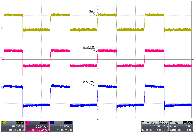
GUID-20220531-SS0I-C14B-C29N-KQBHTBMSBNML-low.pngFigure 3-10 LM5002, 9-V Input, 12-V Positive and Negative Dual-Output Power Supply Switch Nodes