SBAA531 November 2021 ADS8860 , ADS8862 , ADS8881 , ADS9110 , ADS9224R
- Trademarks
- 1Introduction
-
2
Internal Topology of SAR ADC Model
- 2.1 Sample and Hold
- 2.2 Sample and Hold Timing
- 2.3 Reference Transients
- 2.4 Bandwidth Modeling
- 2.5 Noise Modeling
- 2.6 Reference Droop and Reference Noise Errors
- 2.7 Gain, Offset, and Input Leakage Modeling
- 2.8 Differential input behavior
- 2.9 ESD Protection Diodes and Parasitic Capacitance
- 2.10 Summary of Parameters
- 2.11 Summary of Model Pins
- 3Downloading and Using PSpice® Example Projects From Web
- 4Summary
2.3 Reference Transients
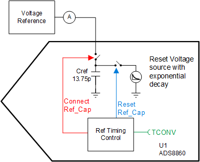
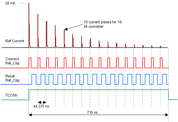
The reference input to many SAR ADCs is not a high impedance. This input has a switched capacitor input that can have multiple large transient currents over a short duration of time. In fact, the number of transients is typically equal to the device resolution, and these transients are spread equally across the conversion phase. So, a 16-bit converter with a 710-ns conversion phase has 16 transient pulses across the 710-ns conversion (710 ns / 16 = 44.375 ns between pulses). The average current for all these current pulses is generally provided in the data sheet. For each conversion phase, the magnitude of the current pulses starts large then diminishes throughout the conversion cycle. This model has parameters for the average reference current (Iref), the number of pulses (N), the reference value (Vref), and the sampling rate (Fsampl). All these parameters are used to generate the transient current waveform on the reference input. For example, the ADS8860 is a 16-bit converter with a 5-V reference that draws an average reference current of 300 μA at a sampling rate of 1 Msps so the parameters are set as follows: Iref = 300 μA, N = 16, Fsampl = 1 MHz, and Vref = 5 V. These parameters are applied to modeling equations that select the appropriate switching capacitor which generates the current transient waveform. The model uses timing control circuits to charge the Cref capacitor and to connect and disconnect the capacitor N number of times. In between each connection, the capacitor is reset to the appropriate voltage to generate the average current. Note that this exponential decay of the transient level approximates what happens in the real-world circuit. The real-world circuit transient level diminishes as shown in the simulation but also has some dependency on the input signal. Nevertheless, from a practical perspective the exponential decay of the transients is sufficient for accurate simulation results.
Figure 2-3 illustrates a simplified version of this circuit, and Figure 2-4 shows an example of the reference current for ADS8860.
 Figure 2-3 Reference Transient Current
Block Diagram
 Figure 2-4 Reference Current Waveform for
ADS8860