SBAA531 November 2021 ADS8860 , ADS8862 , ADS8881 , ADS9110 , ADS9224R
- Trademarks
- 1Introduction
-
2
Internal Topology of SAR ADC Model
- 2.1 Sample and Hold
- 2.2 Sample and Hold Timing
- 2.3 Reference Transients
- 2.4 Bandwidth Modeling
- 2.5 Noise Modeling
- 2.6 Reference Droop and Reference Noise Errors
- 2.7 Gain, Offset, and Input Leakage Modeling
- 2.8 Differential input behavior
- 2.9 ESD Protection Diodes and Parasitic Capacitance
- 2.10 Summary of Parameters
- 2.11 Summary of Model Pins
- 3Downloading and Using PSpice® Example Projects From Web
- 4Summary
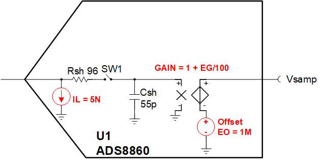
2.7 Gain, Offset, and Input Leakage Modeling
The input voltage offset is modeled by placing a DC voltage source in series with the input. The leakage currents are modeled as DC current sources on each input. Gain error is modeled as a voltage-controlled voltage source with a gain that includes the error (GAIN = 1 + EG / 100). Figure 2-9 illustrates the gain, offset, and leakage modeling.
 Figure 2-9 Reference Noise Scaling
Model