SBAA531 November 2021 ADS8860 , ADS8862 , ADS8881 , ADS9110 , ADS9224R
- Trademarks
- 1Introduction
-
2
Internal Topology of SAR ADC Model
- 2.1 Sample and Hold
- 2.2 Sample and Hold Timing
- 2.3 Reference Transients
- 2.4 Bandwidth Modeling
- 2.5 Noise Modeling
- 2.6 Reference Droop and Reference Noise Errors
- 2.7 Gain, Offset, and Input Leakage Modeling
- 2.8 Differential input behavior
- 2.9 ESD Protection Diodes and Parasitic Capacitance
- 2.10 Summary of Parameters
- 2.11 Summary of Model Pins
- 3Downloading and Using PSpice® Example Projects From Web
- 4Summary
1 Introduction
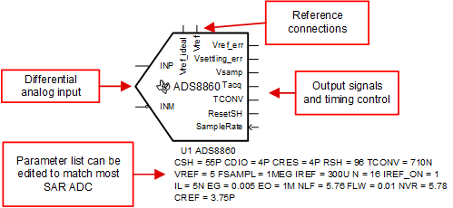
This document describes the operation and design of a flexible Successive Approximation Register (SAR) Analog to Digital Converter (ADC) model. The model was developed to be easily modifiable using SPICE parameters so that it can be used for simulating the behavior of many different SAR ADCs. By adjusting the parameters, this behavioral model can be modified to cover many different models of SAR ADCs. This document defines each parameter and shows how the parameter value can be determined from the device data sheet. Thus, if a model for a particular device is not available, the general model can be modified to cover most ADCs. Figure 1-1 shows the spice model with its associated parameter list. Various performance criteria such as input switching transients, noise, and offset can be modified by adjusting the model parameters. The first part of this document covers the internal operation of the model and how the external parameters can be set using data sheet criteria. The second part of this document covers ADC design optimization using the model. The final part of this document covers design performance verification using the model.
 Figure 1-1 ADC Model With Parameters