SBAA531 November 2021 ADS8860 , ADS8862 , ADS8881 , ADS9110 , ADS9224R
- Trademarks
- 1Introduction
-
2
Internal Topology of SAR ADC Model
- 2.1 Sample and Hold
- 2.2 Sample and Hold Timing
- 2.3 Reference Transients
- 2.4 Bandwidth Modeling
- 2.5 Noise Modeling
- 2.6 Reference Droop and Reference Noise Errors
- 2.7 Gain, Offset, and Input Leakage Modeling
- 2.8 Differential input behavior
- 2.9 ESD Protection Diodes and Parasitic Capacitance
- 2.10 Summary of Parameters
- 2.11 Summary of Model Pins
- 3Downloading and Using PSpice® Example Projects From Web
- 4Summary
2.1 Sample and Hold
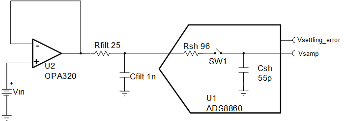
A SAR ADC operates by sampling the input signal during the acquisition period and holding the signal during the conversion period. The sampling action is performed during the acquisition period by closing switch SW1 and allowing sampling Csh to charge via resistor Rsh. At the end of the acquisition period, the switch is opened and the input voltage is held for conversion. To achieve minimal distortion, the capacitor Csh needs to be fully settled at the end of the acquisition phase to properly measure the externally applied signal. The settling is dependent on amplifier bandwidth, the external RC filter, the internal sampling circuit, and the ADC timing. The model has a Vsamp output that shows the sampling behavior, and a Vsettling_error output that displays the difference between the sampled value and the steady state input signal. This settling analysis can be used to facilitate the selection of the amplifier and optimization of the external RC circuit. An input drive circuit optimization is covered in detail in Section 3.1. Figure 2-1 illustrates the ADC system design with the internal sample and hold circuit. Note that Rsh and Csh are parameters that can be adjusted according to the ADC data sheet. Most SAR ADC data sheets provide an input sampling stage equivalent circuit. This circuit provides values for Rsh and Csh.
 Figure 2-1 ADC System Showing External
Drive Circuit and Internal Sample and Hold