SBOA620 March 2025 TMCS1126 , TMCS1126-Q1 , TMCS1133 , TMCS1133-Q1
3.1.1 Components for Differential-Mode Noise Reduction
The highlighted components in Figure 3-3 are required to reduce DM noise on the given pin of the device. Ferrite beads L1, L2, L4, and L5 serve to create high-impedance pathways between the system traces and the device, discouraging noise away from these traces. For the portion that does travel into the local area of the TMCS112x/3x, capacitors C3, C4, and C7 form low pass filters with these components to shunt away the noise before reaching the device.
Note that the TMCS112x/3x has data sheet limits on the amount of capacitance able to be supported by the VOUT and VREF pins of 4.7nF and 20nF, respectively, that must be adhered to. Resistor R1 serves as an optional isolation resistor to bolster the output impedance of the output pin, allowing for capacitance greater than 4.7nF to be used (by default this is set to 0Ω to simply pass the VOUT signal out from the device). Care must be taken when populating R1 with a non-zero value, as this can form a low pass filter with the device's output, and potentially reduce the bandwidth of the device. Filter design can also be affected, and this component need to be modeled if used.
 Figure 3-3 Components for
Differential-Mode Noise Reduction
Figure 3-3 Components for
Differential-Mode Noise ReductionResistor R2 is placed for resonance reasons. As an example, assume noise signatures are identified in the system at a frequency 2.62MHz. The measurements made show up to 1Vpp noise present on the output pin of the TMCS112x/3x for this given frequency, and the design goal is to reduce this to less than 200mVpp. In dB, this can equate to a 14dB attenuation as shown in Equation 1.
These values are summarized in Table 3-1.
| Frequency (MHz) | Measured Noise (Vpp) | Target Attenuation (dB) |
|---|---|---|
| 2.62 | 1 | 14 |
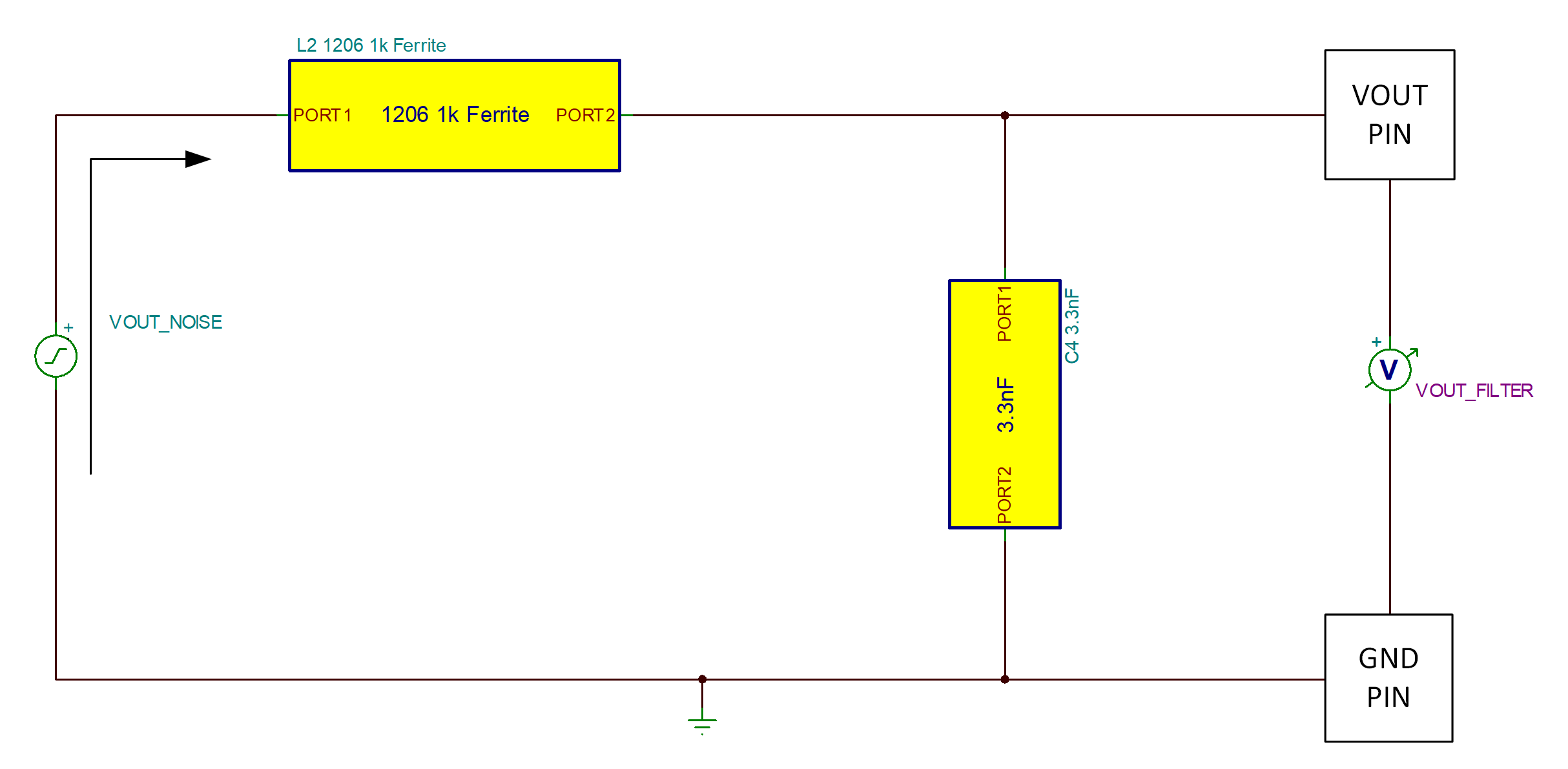
Several tools exist to help achieve these types of designs, such as Murata's Sim-Surfing suite of filter design tools. A 3.3nF capacitor is chosen to make sure the data sheet limit for the VOUT pin is met, and then an appropriate ferrite was determined. Upon choosing components, simulations were performed as shown in Figure 3-4 and Figure 3-5. While the ferrite and capacitor yield the desired -40dB/decade attenuation, can be observed that a resonance has formed between these components and a near 40x gain has been formed at 1.24MHz. This resonance results in a failure to obtain the desired attenuation at 2.62MHz.
Resistor R2 is then placed in the system. This resistor serves to dampen the resonance between these components. Figure 3-6 and Figure 3-7 show the re-run simulation with resistor populated. The observation is that placement of the resistor eliminates the resonant peak from the response, and also corrects the attenuation into acceptable limits. The 40dB attenuation also removes additional high frequency content from the response out to approximately 150Mhz.
 Figure 3-4 DM Filter Modeling of VOUT
pin, R2 not Populated
 Figure 3-6 DM Filter Modeling of VOUT
pin, R2 Populated
 Figure 3-5 DM Filter Simulation
Results, VOUT pin, R2 not Populated
 Figure 3-7 DM Filter Simulation
Results, VOUT pin, R2 Populated