SLAA988A December 2020 – January 2022 TAS2563
1.8 Output Pins
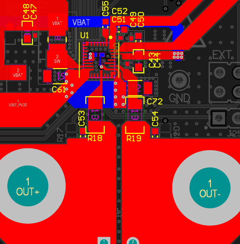
OUT_N and OUT_P are the Class-D channel negative and positive output, respectively. Due to its switching nature, TI recommends keeping the routing short to limit the emissions.
For optimal current flow, the PCB traces must be widened near to the output pins. In addition, the outputs need to be routed on two layers using several vias to minimize parasitic impedance.
It is important to consider a few things when using an EMI filter (LC array):
Inductance should be the first element in the filter.
Capacitance to GND or other output will pull high-current spikes capable of triggering overcurrent protection.
TI recommends fixing 1.5 MHz as the lower limit of the corner frequency to simplify the filter debug and noise issues.
Place 1kΩ resistors in series to VSNS pins to prevent higher current spikes damaging the sense pins internal structure.
 Figure 1-10 OUT_P and OUT_N Connections