SLAA988A December 2020 – January 2022 TAS2563
1.10 Digital Portion
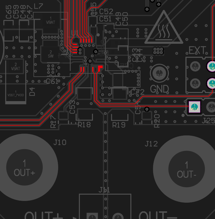
The TAS2563 device involves digital and analog activity. Care must be taken when routing the different signals since it may result in noise issues, especially from the digital lines to the analog portion.
The digital lines can reach frequencies up to 1 MHz for the I2C lines in Fast-Mode Plus and up to 50 MHz for the I2S lines. This high-frequency content can affect the performance of the analog signals. For measurement purposes, the digital noise level may affect the scope captures or a THD+N measurement.
 Figure 1-12 Digital Conections