SLAA988A December 2020 – January 2022 TAS2563
1.1 Typical Application Circuit
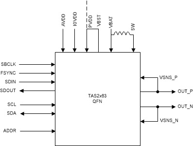
Figure 1-1 shows the typical application block diagram for TAS2563 device.
 Figure 1-1 TAS2x63 Block Diagram
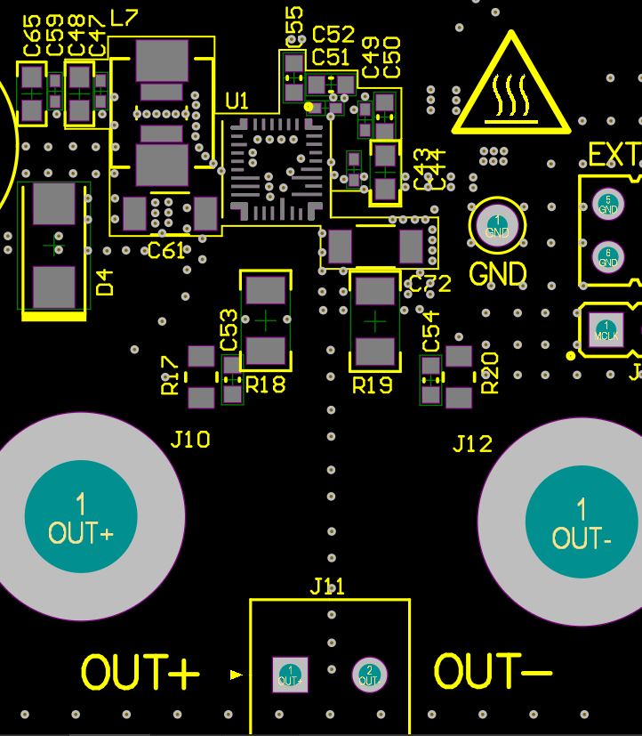
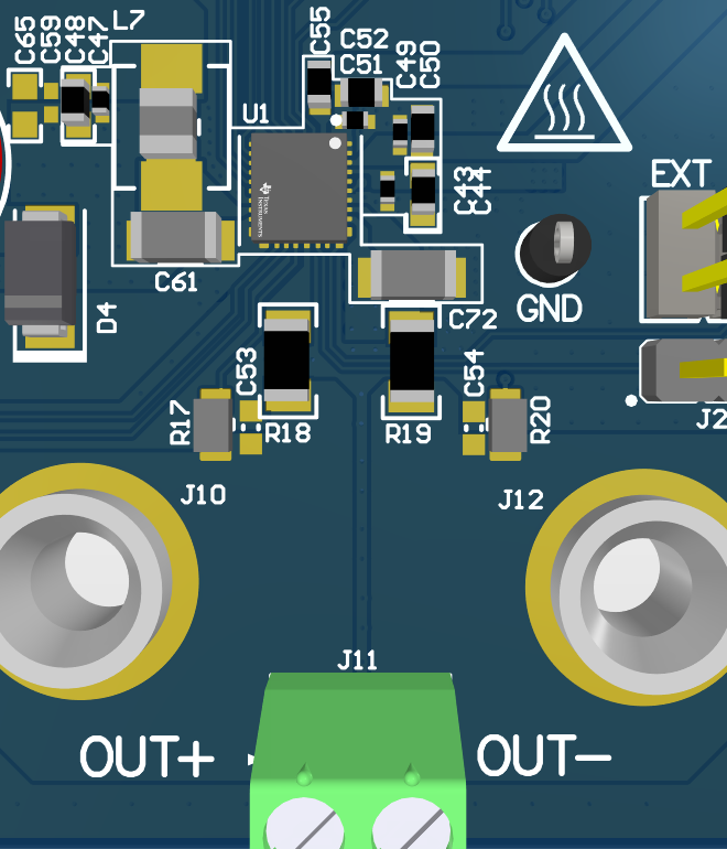
Figure 1-2 and Figure 1-3 show the components location of the PCBA reference layout.
 Figure 1-2 TAS2x63EVM Component Locations
 Figure 1-3 TAS2x63EVM Component Locations (3D View)