SLAA988A December 2020 – January 2022 TAS2563
1.5 PVDD and VBST
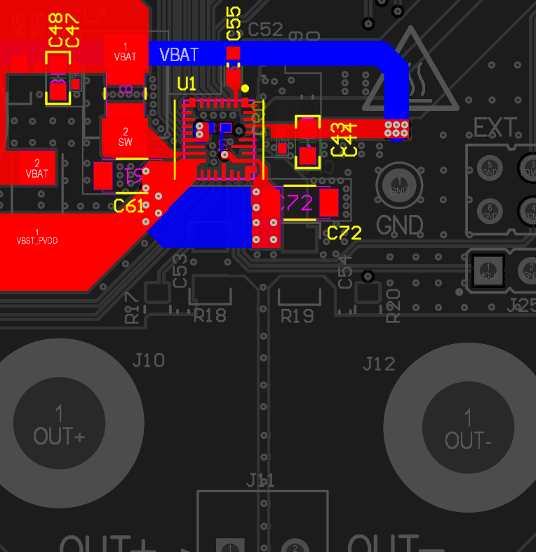
VBST is the internal boost converter output. This is the pin that will supply the power stage supply pin (PVDD). PVDD must be shorted to the VBST pin using a strong connection.
There are a few considerations that must be taken into account for the PVDD to VBST connection:
VBST must not be connected to an external load. This pin should be bypassed to GND with decoupling capacitors. The decoupling capacitor ends should see as low an inductance as possible between the VBST pin and the BGND pin. See the LINK for details.
There should be a maximum parasitic inductance of 100 pH from the device pin to decoupling.
VBST should be connected to PVDD through a thick plane (use multiple vias to reduce parasitic inductance).
PVDD should be connected with a star connection to the GREG capacitor.
VBST and PVDD traces carry a high amount of current. The traces should support currents up to the device overcurrent limit.
Boost capacitor derating should satisfy the ratio with boost inductor: L/C < 1/3 • Ceramic capacitors derate with the applied DC voltage. Often, a 10-µF capacitor loses 80% of the nominal value at the 10-V to 12-V range (for example, a 10-µF capacitance value would result in 2 µF). Typically, TI recommends using a 20-µF capacitor (or a pair of two 10-µF capacitors) as decoupling capacitor.
 Figure 1-7 PVDD and VBST Connection