SLAA988A December 2020 – January 2022 TAS2563
1.4 GREG
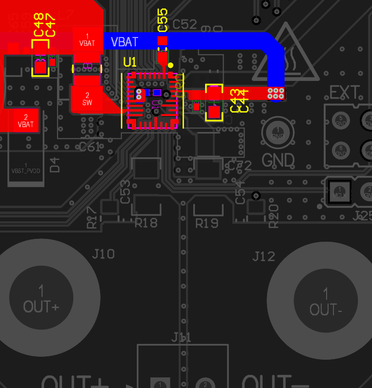
The GREG pin is the output of the high-side gate charge-pump regulator. This pin must not be connected to an external load. A minimum of a 0.1-µF capacitor must be connected from the GREG pin to the PVDD pin (see Figure 1-6, for details).
TI recommends verifying that the PCB design does not generate a parasitic inductance higher than 200 pH. In addition, it is important to connect the GREG pin capacitor to PVDD with a star connection and not to the boost plane. This practice reduces the possibility of EMI radiation.
Similar to the ground pin connections, the layer changes should use multiple vias to minimize the parasitic inductance.
 Figure 1-6 GREG Connection