SLLA497 September 2020 TMS320F28P550SG , TMS320F28P550SJ , TMS320F28P559SG-Q1 , TMS320F28P559SJ-Q1
2.1 Power Stage in a Fast DC Charger
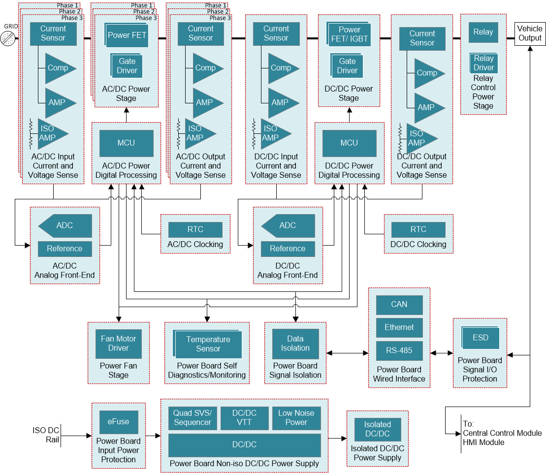
Figure 2-1 shows the system level block diagram of a EV charging station power module captured from TI's EV charging station power module, web page. On the input side it has three-phase AC mains which are connected to the AC/DC power stage. This block converts the incoming AC voltage into a fixed DC voltage of around 800 V. This voltage serves as input to the DC/DC power stage which processes power and interfaces directly with the battery on the electric vehicle.
 Figure 2-1 EERD of EV Charging Station
Power Module.
 The gate drivers driving the power stage MOSFETs also form part of the power stage. In addition to the power stage, current and voltage sensing blocks are available at the input and output of both stages. This is primarily used for control, monitoring, and protection purposes. Each power stage has a separate controller which is responsible for the processing of analog signals and providing fast control action. Apart from this, there are different blocks for temperature sensing, interface for CAN, Ethernet, and RS-485, and isolated and non-isolated DC/DC converters powering the auxiliary circuits like fans for cooling the heat sinks, isolated amplifiers, and so forth. The focus on the remainder of this application report is on the choice of topology for the AC/DC and DC/DC power conversion stage.