SLUUCC4A October   2020  – September 2021 TPS92520-Q1


  1.   Trademarks
  2.   General Texas Instruments High Voltage Evaluation (TI HV EMV) User Safety Guidelines
  3. 1Description
    1. 1.1 Typical Applications
    2. 1.2 Warnings
    3. 1.3 Connector Description
  4. 2Performance Specifications
  5. 3Performance Data and Typical Characteristic Curves
    1. 3.1 1.5A CC BUCK SW-Node Voltage Waveform
    2. 3.2 Start-up Waveforms
    3. 3.3 PWM Dimming
  6. 4Schematic, PCB Layout, and Bill of Materials
    1. 4.1 Schematic
    2. 4.2 Layout
    3. 4.3 Bill of Materials
  7. 5Software
    1. 5.1 Demonstration Kit Software Installation for LEDMCUEVM-132 Board
      1. 5.1.1 Installation Overview
    2. 5.2 Step-by-Step Installation Instructions
    3. 5.3 Installation Error Recovery
    4. 5.4 Checking for Updates
  8. 6TPS92520EVM-133 Power Up and Operation
    1. 6.1 Power Up and Operation at VINx < 40 V
    2. 6.2 MCU Control Window
    3. 6.3 SPI Command Window
    4. 6.4 Watchdog Window
    5. 6.5 GUI Devices Window
      1. 6.5.1 Channel 1 or 2 Sub-Window: Settings, Measurements, and Faults
      2. 6.5.2 Device Sub-Window: Shared Device Settings, Measurements, Register Info, and Limp Home
    6. 6.6 Limp Home Mode Window
  9. 7Revision History

1.5A CC BUCK SW-Node Voltage Waveform

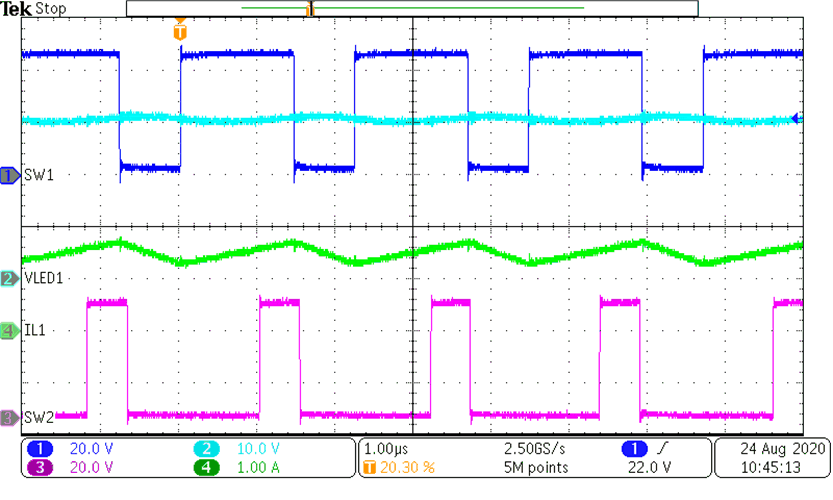
Figure 3-1 shows the switch node voltage waveforms of the channel 1 and channel 2 of the TPS92520EVM-133 dual channel BUCK LED driver. The switch node (SW1 and SW2) of the two channels that are completely independent of each other. SW1 and SW2 are not in phase and are not 180 degrees out of phase. The switching frequency, input voltage, and out LED current setpoints can also be set independently on each channel.
GUID-20200824-CA0I-XXHD-8XXW-BQHZPGJLJ5SP-low.gif
VIN = 48 V, VLED1 = 30 V, VLED2 = 10 V
Figure 3-2 Dual-Channel Buck SW-Node Voltage