SLVAEW7 September 2020 ADC12DJ5200RF , LMK00304 , LMK04828 , LMX2594 , TPS62912 , TPS62913
1.1.1 ADC12DJ5200 Noise and Ripple Requirements
The ADC12DJ5200RF is a 12bit GSPS RF-analog-to-digital converter (ADC) that can directly sample input frequencies from DC to above 8GHz. ADC12DJ5200RF can be configured as a dual-channel, 5.2 GSPS ADC or single-channel, 10.4 GSPS ADC. These operating modes allow programmable tradeoffs in channel count and Nyquist bandwidth. Useable input frequency range of up to 8 GHz enables direct RF sampling of L-band, S-band, C-band, and X-band for frequency agile systems. The ADC12DJ5200RF uses a high-speed JESD204C output interface with up to 16 serialized lanes supporting up to 17.16 Gbps line rate. Deterministic latency and multi-device synchronization is supported through JESD204C subclass-1. The interface is backwards compatible with JESD204B receivers. Innovative synchronization features, including noiseless aperture delay (TAD) adjustment and SYSREF windowing, simplify system design for multichannel applications. Optional digital down converters (DDCs) are available to provide digital conversion to baseband and to reduce the interface rate. A programmable FIR filter allows on-chip equalization.
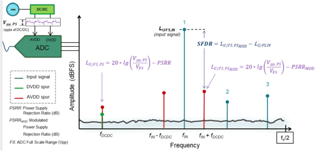
The original product evaluation module (EVM) implements low-noise LDOs in addition to the DC/DC buck regulators to minimize any impairments from the supply network. While the DC accuracy of the supply rail is specified for the ADC12DJ5200RF, there is no specification on supply voltage noise and supply voltage ripple. Any supply ripple or noise appears attenuated on the output spectrum of the ADC. This attenuation can be expressed as Power Supply Rejection Ration (PSRR) and PSRRMOD (or PSMR) as shown in Figure 1-1.
 Figure 1-1 Power supply noise and ripple
in the ADC output spectrum
Figure 1-1 Power supply noise and ripple
in the ADC output spectrumPSRR is the attenuation of the ADC input supply ripple to the ADC output spectrum at the switching frequency fundamental of the DC-DC converter (fDCDC). PSRRMOD (or PSMR) is the attenuation from the ADC input to the modulated spur in the output spectrum (fin - fDCDC, fin + fDCDC).
PSRR is usually less of a concern since it is typically >40 dB and outside of the frequency of interest, however some analog rails can have PSRR of <40 dB, as shown in Figure 1-2, which shows the most sensitive supplies of the ADC12DJ5200RF are the analog supply rails of VA11 and VA19. More important is PSMR, since the attenuation from the supply rail to the modulated spur can be low for sensitive analog rails such as VA11 and VA19 on the ADC12DJ5200RF.
 Figure 1-2 ADC12DJ5200 PSRR of the VA11, VD11, and VA19 Supplies