SLVUCA1 November   2021 TPS7H1210-SEP


  1.   Trademarks
  2. 1Introduction
    1. 1.1 Features
    2. 1.2 Applications
  3. 2Setup
    1. 2.1 Input/Output Connectors and Jumper Descriptions
      1. 2.1.1 J1, J4 (–)VIN
      2. 2.1.2 J6 GND
      3. 2.1.3 J2, J5 (–)VOUT
      4. 2.1.4 J7 GND
      5. 2.1.5 J3 EN
      6. 2.1.6 TP1-5 Test Points
    2. 2.2 Equipment Setup
  4. 3Operation
  5. 4Adjustable Operation
  6. 5Test Results
    1. 5.1 Enable, Disable, and Soft Start Timing
    2. 5.2 Output Load Transients
    3. 5.3 PSRR
    4. 5.4 Noise Spectral Density
  7. 6Board Layout
  8. 7Schematic and Bill of Materials

Output Load Transients

Figure 5-2 shows the load transient response (Chan 2 VOUT, red) for a load step transient from 1 mA to 500 mA (Chan 4 VIN, purple). The TPS7H1210EVM was operating at stock configuration with VIN = –6 V, VOUT = –5 V. Figure 5-2 shows the load transient from 500 mA to 1 mA.
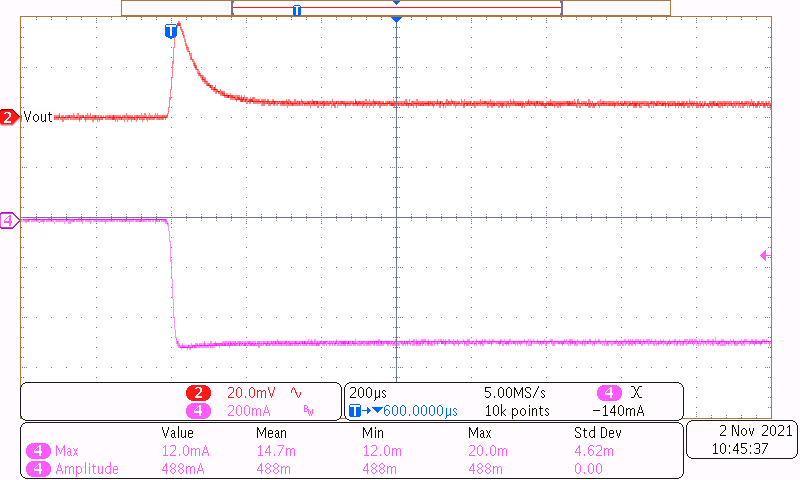
GUID-20211104-SS0I-J438-CJQ0-SPV9TGSTGKWQ-low.png Figure 5-2 Load Step Transient Response Rising
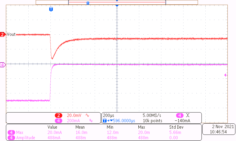
GUID-20211104-SS0I-RGL8-RXNX-HGR9DFF9GJ9K-low.png Figure 5-3 Load Step Transient Response Falling