SLVUCA1 November   2021 TPS7H1210-SEP


  1.   Trademarks
  2. 1Introduction
    1. 1.1 Features
    2. 1.2 Applications
  3. 2Setup
    1. 2.1 Input/Output Connectors and Jumper Descriptions
      1. 2.1.1 J1, J4 (–)VIN
      2. 2.1.2 J6 GND
      3. 2.1.3 J2, J5 (–)VOUT
      4. 2.1.4 J7 GND
      5. 2.1.5 J3 EN
      6. 2.1.6 TP1-5 Test Points
    2. 2.2 Equipment Setup
  4. 3Operation
  5. 4Adjustable Operation
  6. 5Test Results
    1. 5.1 Enable, Disable, and Soft Start Timing
    2. 5.2 Output Load Transients
    3. 5.3 PSRR
    4. 5.4 Noise Spectral Density
  7. 6Board Layout
  8. 7Schematic and Bill of Materials

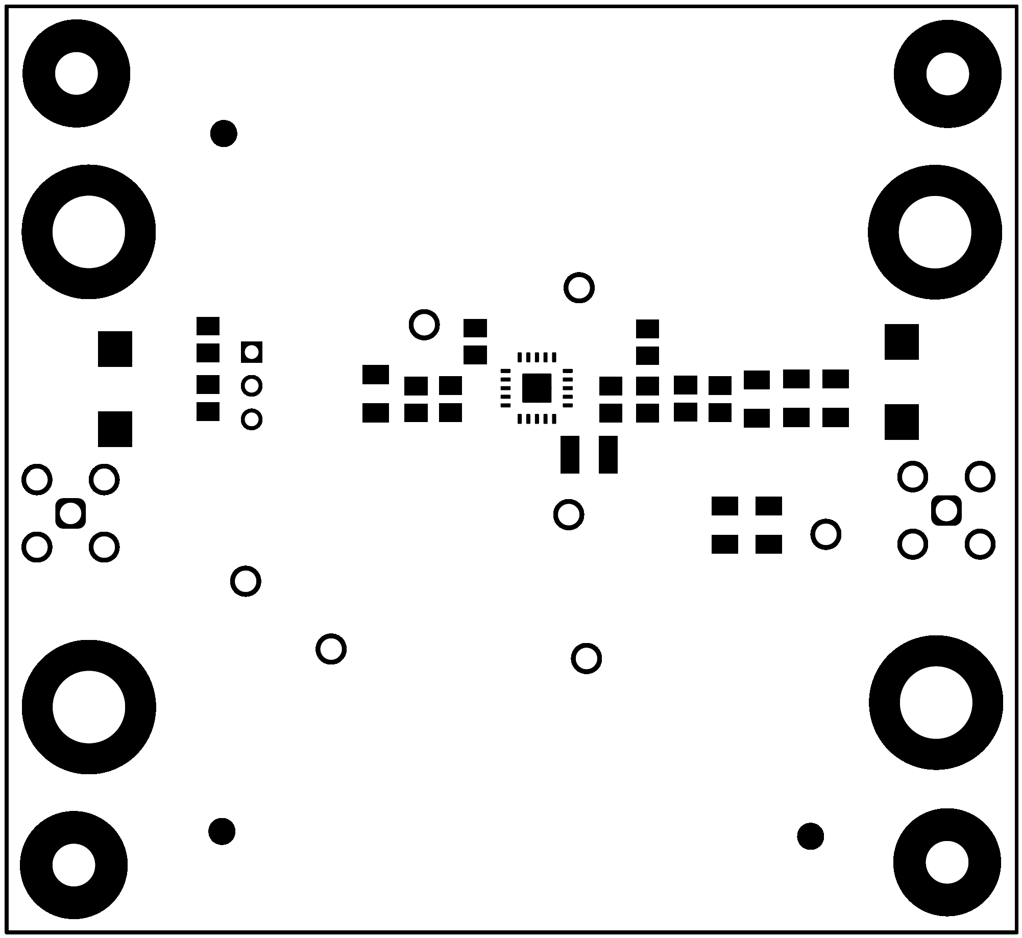
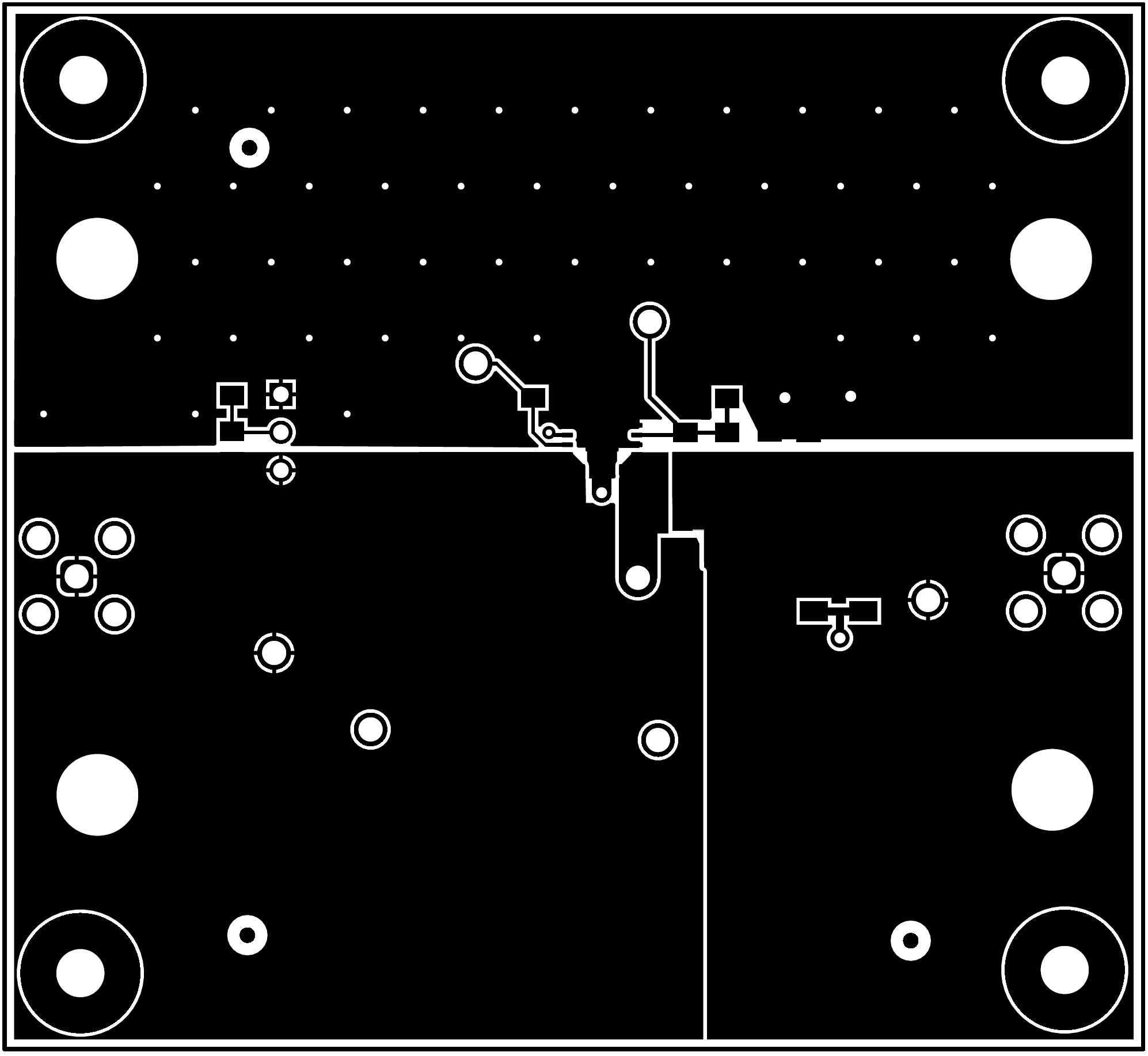
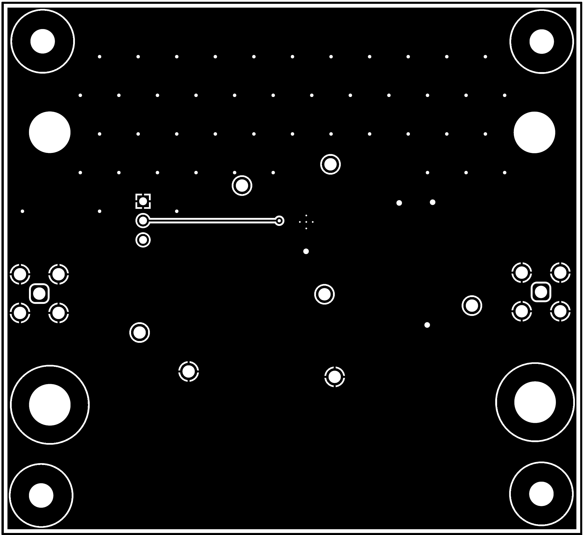
Board Layout

The following images represent the board design layers.
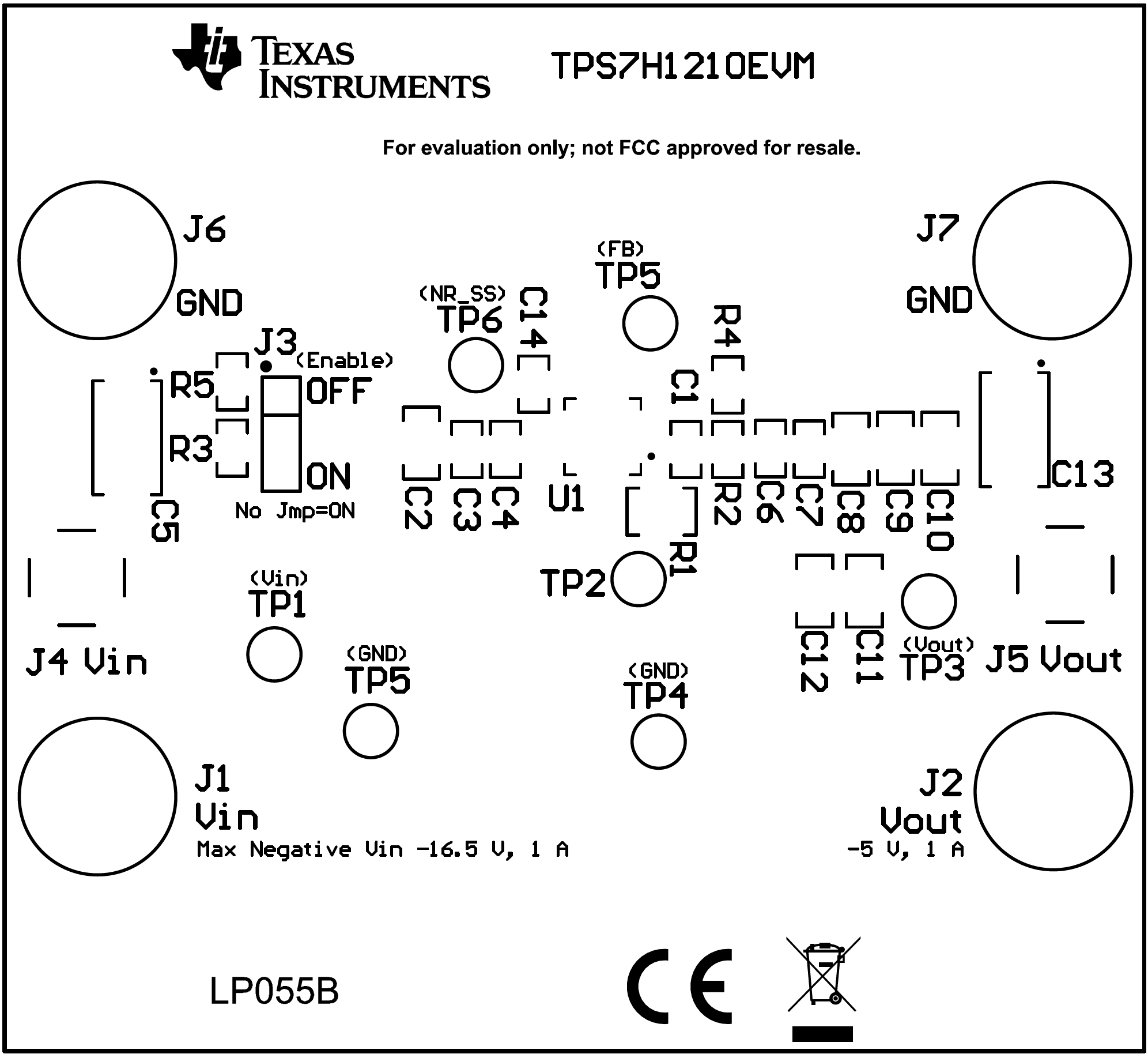
GUID-20211104-SS0I-LNDD-3LZZ-GKGJ5G4WHLMZ-low.png Figure 6-1 Top Overlay Silkscreen
GUID-20211104-SS0I-M3DF-C5X2-XD9SDNZFZNTS-low.png Figure 6-2 Top Solder Mask
GUID-20211104-SS0I-6W9R-WMBK-X8WFVQFCSQ1J-low.png Figure 6-3 Top Signal Layer
GUID-20211104-SS0I-SVXL-8K8G-DTWCH0HHS42N-low.png Figure 6-4 Bottom Signal Layer