SLWU086C November 2013 – January 2016 ADS42JB46 , ADS42JB49 , ADS42JB69 , DAC38J84
1 Functionality
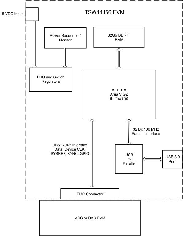
The TSW14J56EVM has a single industry standard FMC connector that interfaces directly with TI JESD204B ADC and DAC EVM's. When used with an ADC EVM, high-speed serial data is captured, de-serialized and formatted by an Altera Arria V GZ FPGA. The data is then stored into an external DDR3 memory bank, enabling the TSW14J56 to store up to 2G 16-bit data samples. To acquire data on a host PC, the FPGA reads the data from memory and transmits it on a high speed 32 bit parallel interface. An onboard high-speed USB 3.0 to parallel converter bridges the FPGA interface to the host PC and GUI.
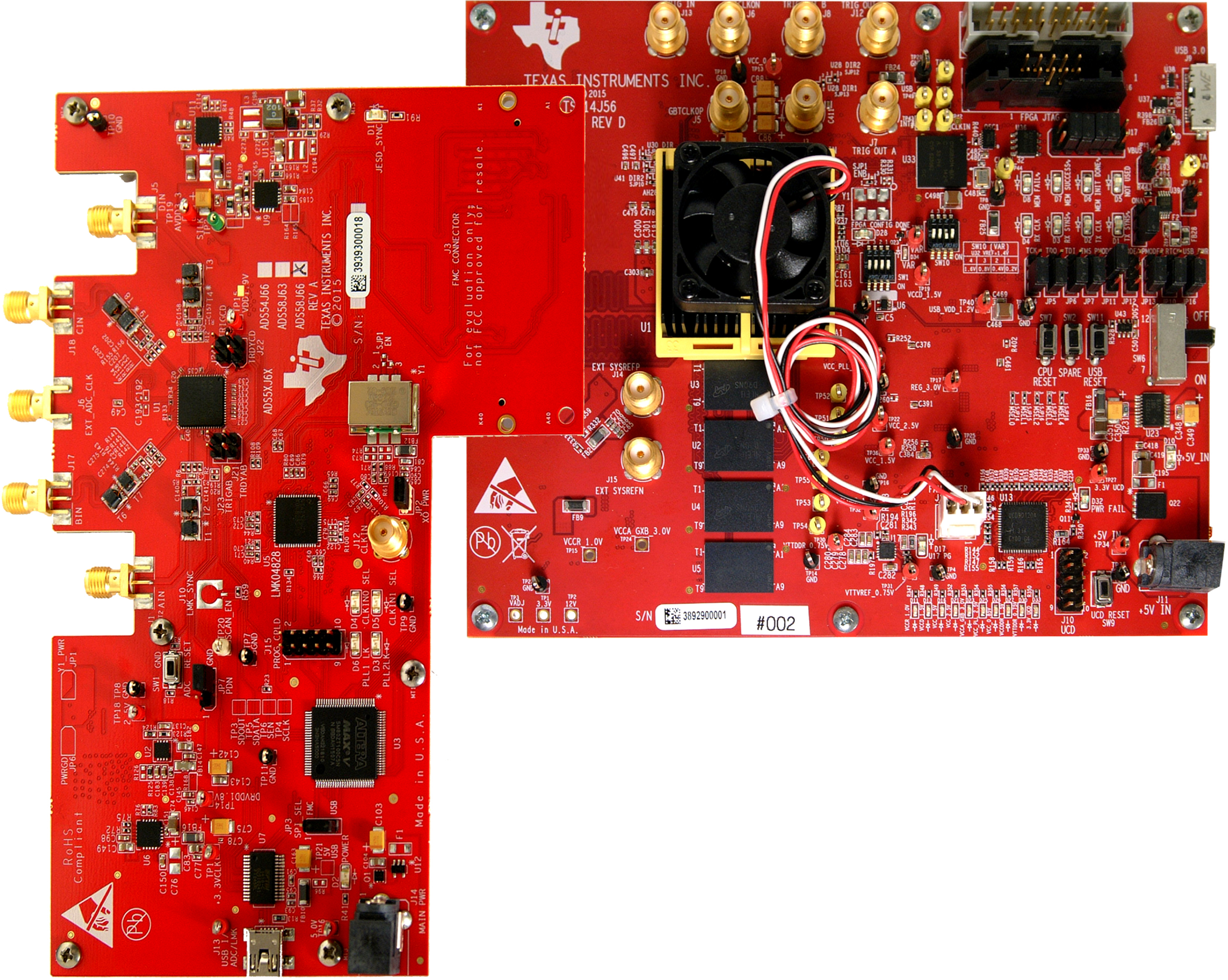
In pattern generator mode, the TSW14J56 generates desired test patterns for DAC EVMs under test. These patterns are sent from the host PC over the USB interface to the TSW14J56. The FPGA stores the data received into the board DDR3 memory module. The data from memory is then read by the FPGA and transmitted to a DAC EVM across the JESD204B interface connector. The board contains a 100-MHz oscillator used to generate the DDR3 reference clock and a option for a 10-MHz oscillator for general purpose use. Figure 1 shows the TI ADS58J63EVM plugged into the TSW14J56EVM.
The major features of the TSW14J56 are:
- Subclasses: 0 (backward compatible), 1, 2
- Support for deterministic latency
- Serial lanes speeds up to 12.5 Gbps
- 10 routed transceiver channels
- 32 Gb DDR3 SDRAM (split into four independent 512×164 Gb SDRAMs, total of 512M samples each). Quarter rate DDR3 controllers supporting up to 800-MHz operation
- 256K 16-bit samples of internal FPGA memory
- Supports 1.8, 2.5 and 3-V adjustable CMOS IO standard
- Option for general purposed 10 MH oscillator
- Onboard UCD90120A for power sequencing and monitoring
- Onboard Cypress CYUSB301X USB 3.0 device for JTAG and parallel interface to the FPGA
- Reference clocking for transceivers available through FMC port or SMAs
- Supported by TI HSDC PRO software
- FPGA firmware developed with Quartus II 14.0 and QSYS
- JESD RX IP core with support for:
- USB and JTAG reconfigurable JESD core parameters: L, M, K, F, HD, S, and more
- ILA configuration data accessible through USB and JTAG
- Lane alignment and character replacement enabled or disabled through USB and JTAG
- JESD TX IP core with support for:
- USB and JTAG reconfigurable JESD core parameters: L, M, K, F, HD, S, and more
- ILA data configured through USB and JTAG
- Character replacement enabled or disabled through USB and JTAG
- Dynamically reconfigurable transceiver data rate. Operating range from 0.600 to 12.5 Gbps
- JESD RX IP core with support for:
Figure 2 shows a block diagram of the TSW14J56 EVM.

