SNVA994A February 2022 – March 2023 LM5157 , LM5157-Q1 , LM51571-Q1 , LM5158 , LM5158-Q1 , LM51581 , LM51581-Q1
- 1
- Trademarks
- 1Introduction
- 2Example Application
- 3Calculations and Component Selection
- 4Component Selection Summary
- 5Small Signal Frequency Analysis
- 6Revision History
3.8 Control Loop Compensation
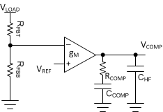
One benefit of the peak current mode control is the easier compensation design compared with that of the voltage mode control. A simple two-pole (one at origin), single zero network is adequate. A type II compensation network is implemented as shown in Figure 3-1, which provides a programmable zero and a pole. The following section introduces a general technique to set the crossover frequency and place the pole and zero of the error amplifier to achieve a stable system in the CCM for a primary side regulated Flyback. The detailed models of the control loop are presented in Section 5. An example for the compensation of an isolated Flyback can be found in How to Design an Isolated Flyback using LM5155 application note.
 Figure 3-1 Type II Compensation Network