SPRAC21A June   2016  – June 2019 OMAP-L132 , OMAP-L138 , TDA2E , TDA2EG-17 , TDA2HF , TDA2HG , TDA2HV , TDA2LF , TDA2P-ABZ , TDA2P-ACD , TDA2SA , TDA2SG , TDA2SX , TDA3LA , TDA3LX , TDA3MA , TDA3MD , TDA3MV


  1.   TDA2xx and TDA2ex Performance
    1.     Trademarks
    2. SoC Overview
      1. 1.1 Introduction
      2. 1.2 Acronyms and Definitions
      3. 1.3 TDA2xx and TDA2ex System Interconnect
      4. 1.4 Traffic Regulation Within the Interconnect
        1. 1.4.1 Bandwidth Regulators
        2. 1.4.2 Bandwidth Limiters
        3. 1.4.3 Initiator Priority
      5. 1.5 TDA2xx and TDA2ex Memory Subsystem
        1. 1.5.1 Controller/PHY Timing Parameters
        2. 1.5.2 Class of Service
        3. 1.5.3 Prioritization Between DMM/SYS PORT or MPU Port to EMIF
      6. 1.6 TDA2xx and TDA2ex Measurement Operating Frequencies
      7. 1.7 System Instrumentation and Measurement Methodology
        1. 1.7.1 GP Timers
        2. 1.7.2 L3 Statistic Collectors
    3. Cortex-A15
      1. 2.1 Level1 and Level2 Cache
      2. 2.2 MMU
      3. 2.3 Performance Control Mechanisms
        1. 2.3.1 Cortex-A15 Knobs
        2. 2.3.2 MMU Page Table Knobs
      4. 2.4 Cortex-A15 CPU Read and Write Performance
        1. 2.4.1 Cortex-A15 Functions
        2. 2.4.2 Setup Limitations
        3. 2.4.3 System Performance
          1. 2.4.3.1 Cortex-A15 Stand-Alone Memory Read, Write, Copy
          2. 2.4.3.2 Results
    4. System Enhanced Direct Memory Access (System EDMA)
      1. 3.1 System EDMA Performance
        1. 3.1.1 System EDMA Read and Write
        2. 3.1.2 System EDMA Results
      2. 3.2 System EDMA Observations
    5. DSP Subsystem EDMA
      1. 4.1 DSP Subsystem EDMA Performance
        1. 4.1.1 DSP Subsystem EDMA Read and Write
        2. 4.1.2 DSP Subsystem EDMA Results
      2. 4.2 DSP Subsystem EDMA Observations
    6. Embedded Vision Engine (EVE) Subsystem EDMA
      1. 5.1 EVE EDMA Performance
        1. 5.1.1 EVE EDMA Read and Write
        2. 5.1.2 EVE EDMA Results
      2. 5.2 EVE EDMA Observations
    7. DSP CPU
      1. 6.1 DSP CPU Performance
        1. 6.1.1 DSP CPU Read and Write
        2. 6.1.2 Code Setup
          1. 6.1.2.1 Pipeline Copy
          2. 6.1.2.2 Pipeline Read
          3. 6.1.2.3 Pipeline Write
          4. 6.1.2.4 L2 Stride-Jmp Copy
          5. 6.1.2.5 L2 Stride-Jmp Read
          6. 6.1.2.6 L2 Stride-Jmp Write
      2. 6.2 DSP CPU Observations
      3. 6.3 Summary
    8. Cortex-M4 (IPU)
      1. 7.1 Cortex-M4 CPU Performance
        1. 7.1.1 Cortex-M4 CPU Read and Write
        2. 7.1.2 Code Setup
        3. 7.1.3 Cortex-M4 Functions
        4. 7.1.4 Setup Limitations
      2. 7.2 Cortex-M4 CPU Observations
        1. 7.2.1 Cache Disable
        2. 7.2.2 Cache Enable
      3. 7.3 Summary
    9. USB IP
      1. 8.1 Overview
      2. 8.2 USB IP Performance
        1. 8.2.1 Test Setup
        2. 8.2.2 Results and Observations
        3. 8.2.3 Summary
    10. PCIe IP
      1. 9.1 Overview
      2. 9.2 PCIe IP Performance
        1. 9.2.1 Test Setup
        2. 9.2.2 Results and Observations
    11. 10 IVA-HD IP
      1. 10.1 Overview
      2. 10.2 H.264 Decoder
        1. 10.2.1 Description
        2. 10.2.2 Test Setup
        3. 10.2.3 Test Results
      3. 10.3 MJPEG Decoder
        1. 10.3.1 Description
        2. 10.3.2 Test Setup
        3. 10.3.3 Test Results
    12. 11 MMC IP
      1. 11.1 MMC Read and Write Performance
        1. 11.1.1 Test Description
        2. 11.1.2 Test Results
      2. 11.2 Summary
    13. 12 SATA IP
      1. 12.1 SATA Read and Write Performance
        1. 12.1.1 Test Setup
        2. 12.1.2 Observations
          1. 12.1.2.1 RAW Performance
          2. 12.1.2.2 SDK Performance
      2. 12.2 Summary
    14. 13 GMAC IP
      1. 13.1 GMAC Receive/Transmit Performance
        1. 13.1.1 Test Setup
        2. 13.1.2 Test Description
          1. 13.1.2.1 CPPI Buffer Descriptors
        3. 13.1.3 Test Results
          1. 13.1.3.1 Receive/Transmit Mode (see )
          2. 13.1.3.2 Receive Only Mode (see )
          3. 13.1.3.3 Transmit Only Mode (see )
      2. 13.2 Summary
    15. 14 GPMC IP
      1. 14.1 GPMC Read and Write Performance
        1. 14.1.1 Test Setup
          1. 14.1.1.1 NAND Flash
          2. 14.1.1.2 NOR Flash
        2. 14.1.2 Test Description
          1. 14.1.2.1 Asynchronous NAND Flash Read/Write Using CPU Prefetch Mode
          2. 14.1.2.2 Asynchronous NOR Flash Single Read
          3. 14.1.2.3 Asynchronous NOR Flash Page Read
          4. 14.1.2.4 Asynchronous NOR Flash Single Write
        3. 14.1.3 Test Results
      2. 14.2 Summary
    16. 15 QSPI IP
      1. 15.1 QSPI Read and Write Performance
        1. 15.1.1 Test Setup
        2. 15.1.2 Test Results
        3. 15.1.3 Analysis
          1. 15.1.3.1 Theoretical Calculations
          2. 15.1.3.2 % Efficiency
      2. 15.2 QSPI XIP Code Execution Performance
      3. 15.3 Summary
    17. 16 Standard Benchmarks
      1. 16.1 Dhrystone
        1. 16.1.1 Cortex-A15 Tests and Results
        2. 16.1.2 Cortex-M4 Tests and Results
      2. 16.2 LMbench
        1. 16.2.1 LMbench Bandwidth
          1. 16.2.1.1 TDA2xx and TDA2ex Cortex-A15 LMbench Bandwidth Results
          2. 16.2.1.2 TDA2xx and TDA2ex Cortex-M4 LMBench Bandwidth Results
          3. 16.2.1.3 Analysis
        2. 16.2.2 LMbench Latency
          1. 16.2.2.1 TDA2xx and TDA2ex Cortex-A15 LMbench Latency Results
          2. 16.2.2.2 TDA2xx and TDA2ex Cortex-M4 LMbench Latency Results
          3. 16.2.2.3 Analysis
      3. 16.3 STREAM
        1. 16.3.1 TDA2xx and TDA2ex Cortex-A15 STREAM Benchmark Results
        2. 16.3.2 TDA2xx and TDA2ex Cortex-M4 STREAM Benchmark Results
    18. 17 Error Checking and Correction (ECC)
      1. 17.1 OCMC ECC Programming
      2. 17.2 EMIF ECC Programming
      3. 17.3 EMIF ECC Programming to Starterware Code Mapping
      4. 17.4 Careabouts of Using EMIF ECC
        1. 17.4.1 Restrictions Due to Non-Availability of Read Modify Write ECC Support in EMIF
          1. 17.4.1.1 Un-Cached CPU Access of EMIF
          2. 17.4.1.2 Cached CPU Access of EMIF
          3. 17.4.1.3 Non CPU Access of EMIF Memory
          4. 17.4.1.4 Debugger Access of EMIF via the Memory Browser/Watch Window
          5. 17.4.1.5 Software Breakpoints While Debugging
        2. 17.4.2 Compiler Optimization
        3. 17.4.3 Restrictions Due to i882 Errata
        4. 17.4.4 How to Find Who Caused the Unaligned Quanta Writes After the Interrupt
      5. 17.5 Impact of ECC on Performance
    19. 18 DDR3 Interleaved vs Non-Interleaved
      1. 18.1 Interleaved versus Non-Interleaved Setup
      2. 18.2 Impact of Interleaved vs Non-Interleaved DDR3 for a Single Initiator
      3. 18.3 Impact of Interleaved vs Non-Interleaved DDR3 for Multiple Initiators
    20. 19 DDR3 vs DDR2 Performance
      1. 19.1 Impact of DDR2 vs DDR3 for a Single Initiator
      2. 19.2 Impact of DDR2 vs DDR3 for Multiple Initiators
    21. 20 Boot Time Profile
      1. 20.1 ROM Boot Time Profile
      2. 20.2 System Boot Time Profile
    22. 21 L3 Statistics Collector Programming Model
    23. 22 Reference
  2.   Revision History

Overview

HDVICP2/IVAHD is TIs second generation Video and Imaging co-processor designed to accelerate the HD Video encoding and decoding. It is a successor to the HDVICP 1.0. Both generations support 4:2:0 Chroma formats only. HDVICP2 is sometimes referred to as IVAHD 1.0. The DM46x devices are some of the SoCs that have HDVICP 1.0.

DM816x, DM814x, DM813x, OMAP4, and OMAP5 are some of the SoCs that have HDVICP 2.0. These different SoCs have varying number of instances of HDVICP2 and operating frequency. For more details, see the device-specific data sheet.

The block diagram of IVAHD is shown in Figure 30.
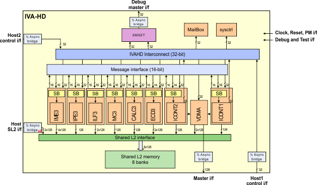
ivahd_bd_sprac21.gifFigure 30. IVAHD Block Diagram

The typical process call structure for the IVAHD codecs that encodes or decodes a single frame of a single channel of encode or decode is shown in Figure 31. The major performance probe points are:

  • Process Call Start – Begin the CODEC operation.
  • HDVICP2 Resource Acquire – Acquire IVAHD resource to start IVAHD operations.
  • HDVICP2 Wait – M4 pre-processing completes. M4 can perform a thread switch to perform some other operation while IVAHD performs encode or decode operations.
  • HDVICP2 Done – M4 receives a completion interrupt from IVAHD and switches back to the codec thread.
  • HDVICP2 Release – M4 post processing thread releases the IVAHD resource.
  • Process Call End – Completion of the frame encodes or decode operation.
ivahd_sw_perf_probe_points.pngFigure 31. IVAHD Software Performance Probe Points