SPRACU1A October 2020 – June 2021 AM2431 , AM2432 , AM2434 , AM6411 , AM6412 , AM6421 , AM6441 , AM6442
- Trademarks
- 1Overview
-
2DDR4 Board Design and Layout Guidance
- 2.1 DDR4 Introduction
- 2.2 DDR4 Device Implementations Supported
- 2.3 DDR4 Interface Schematics
- 2.4 Compatible JEDEC DDR4 Devices
- 2.5 Placement
- 2.6 DDR4 Keepout Region
- 2.7 VPP
- 2.8 Net Classes
- 2.9 DDR4 Signal Termination
- 2.10 VREF Routing
- 2.11 VTT
- 2.12 POD Interconnect
- 2.13 CK and ADDR_CTRL Topologies and Routing Guidance
- 2.14 Data Group Topologies and Routing Guidance
- 2.15 CK and ADDR_CTRL Routing Specification
- 2.16 Data Group Routing Specification
- 2.17 Bit Swapping
-
3LPDDR4 Board Design and Layout Guidance
- 3.1 LPDDR4 Introduction
- 3.2 LPDDR4 Device Implementations Supported
- 3.3 LPDDR4 Interface Schematics
- 3.4 Compatible JEDEC LPDDR4 Devices
- 3.5 Placement
- 3.6 LPDDR4 Keepout Region
- 3.7 Net Classes
- 3.8 LPDDR4 Signal Termination
- 3.9 LPDDR4 VREF Routing
- 3.10 LPDDR4 VTT
- 3.11 CK and ADDR_CTRL Topologies
- 3.12 Data Group Topologies
- 3.13 CK and ADDR_CTRL Routing Specification
- 3.14 Data Group Routing Specification
- 3.15 Channel, Byte, and Bit Swapping
- 4Revision History
2.14 Data Group Topologies and Routing Guidance
Regardless of the number of DDR4 devices implemented, the data line topology is always point-to-point. Minimize layer transitions during routing. If a layer transition is necessary, it is better to transition to a layer using the same reference plane. If this cannot be accommodated, ensure there are nearby ground vias to allow the return currents to transition between reference planes. The goal is to provide a low inductance path for the return current. Also, to optimize the length matching, TI recommends routing all nets within a single data routing group on one layer where all have the exact same number of vias and the same via barrel length.
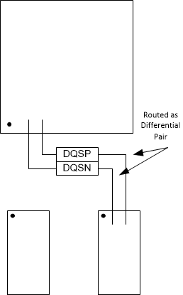
DQSP and DQSN lines are point-to-point signals routed as a differential pair. Figure 2-9 shows the DQS connection topology.
 Figure 2-9 DDR4 DQS Topology
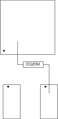
DQ and DM lines are point-to-point signals routed singled-ended. Figure 2-10 shows the DQ and DM connection topology.
 Figure 2-10 DDR4 DQ/DM Topology
Similar to the figures above for the CK and ADDR_CTRL routes, Figure 2-11 and Figure 2-12 show an example of the PCB routes for a DQS routing group and the associated data routing group nets.
The routing example shows DQS0P and DQS0N, which are routed as a differential pair from the processor to the SDRAM that contains Byte 0. This is implemented as a point-to-point routed differential pair without any board terminations. There are no stubs allowed on these nets of any kind. All test access probes must be in line without any branches or stubs. Similar DQS pair routing exists from the processor to each SDRAM for the byte lanes implemented.
Figure 2-12 shows a routing example for a single net in the Byte 0 routing group. The DQ and DM nets are routed single-ended and are also point-to-point without any stubs or board terminations. Point-to-point routes exist for each of the DQ and DM nets implemented.
The DQ and DM nets are routed along the same path as the DQSP and DQSN pair for that byte lane, so that they can be length matched to the DQS pair.
 Figure 2-11 DQS Routing to Two DDR4 SDRAM
Devices
 Figure 2-12 DQ/DM Routing to Two DDR4
SDRAM Devices