SPRUIW7A October   2020  – February 2022


  1.   Trademarks
  2. 1Introduction
    1. 1.1 Key Features
    2. 1.2 Thermal Compliance
    3. 1.3 REACH Compliance
    4. 1.4 Electrostatic Discharge (ESD) Compliance
  3. 2J7200 EVM Overview
    1. 2.1 J7200 EVM Board Identification
    2. 2.2 J7200 SOM Component Identification
    3. 2.3 Jacinto7 Common Processor Component Identification
    4. 2.4 Quad Ethernet Components Identification
  4. 3EVM User Setup/Configuration
    1. 3.1 Power Requirements
    2. 3.2 Power ON Switch and Power LEDs
      1. 3.2.1 Over Voltage and Under Voltage Protection Circuit
      2. 3.2.2 Power Regulators and Power Status LEDs
    3. 3.3 EVM Reset/Interrupt Push Buttons
    4. 3.4 EVM DIP Switches
      1. 3.4.1 EVM Configuration DIP Switch
      2. 3.4.2 SOM Configuration DIP Switch
      3. 3.4.3 Boot Modes
      4. 3.4.4 Other Selection Switches
    5. 3.5 EVM UART/COM Port Mapping
  5. 4J7200 EVM Hardware Architecture
    1. 4.1  J7200 EVM Hardware Top Level Diagram
    2. 4.2  J7200 EVM Interface Mapping
    3. 4.3  I2C Address Mapping
    4. 4.4  GPIO Mapping
    5. 4.5  Power Supply
      1. 4.5.1 Power Sequencing
      2. 4.5.2 Voltage Supervisor
      3. 4.5.3 DDR I/O Voltage Selection
      4. 4.5.4 J7200 SoC SLEEP Logic Operation
      5. 4.5.5 J7200 SoC MCU Only Operation
      6. 4.5.6 J7200 SoC GPIO Retention Operation
      7. 4.5.7 J7200 SoC DDR Retention Operation
      8. 4.5.8 Power Monitoring
      9. 4.5.9 Power Test Points
    6. 4.6  Reset
    7. 4.7  Clock
      1. 4.7.1 Processor’s Primary Clock
      2. 4.7.2 Processor’s Secondary/SERDES Ref Clock
      3. 4.7.3 EVM Peripheral Ref Clock
    8. 4.8  Memory Interfaces
      1. 4.8.1 LPDDR4 Interface
      2. 4.8.2 OSPI Interface
      3. 4.8.3 MMC Interface
        1. 4.8.3.1 MMC0 - eMMC Interface
        2. 4.8.3.2 MMC1 – Micro SD Interface
      4. 4.8.4 Board ID EEPROM Interface
      5. 4.8.5 Boot EEPROM Interface
    9. 4.9  MCU Ethernet Interface
      1. 4.9.1 Gigabit Ethernet PHY Default Configuration
    10. 4.10 QSGMII Ethernet Interface
    11. 4.11 PCIe Interface
      1. 4.11.1 X2 Lane PCIe Interface
    12. 4.12 USB Interface
      1. 4.12.1 USB 3.1 Interface
      2. 4.12.2 USB 2.0 Interface
        1. 4.12.2.1 To PCIe Card Wi-Fi/BT
        2. 4.12.2.2 To Expansion Connector
      3. 4.12.3 USB 3.0 Micro AB Interface (Reserved Port)
    13. 4.13 Audio Interface
      1. 4.13.1 Line IN Port
      2. 4.13.2 MIC Input Port
      3. 4.13.3 Line Out Port
      4. 4.13.4 Head Phone Port
      5. 4.13.5 Port Mapping
    14. 4.14 CAN Interface
      1. 4.14.1 MCU CAN0
      2. 4.14.2 MCU CAN1
      3. 4.14.3 MAIN CAN3 (supports WAKE function)
      4. 4.14.4 MAIN CAN0
    15. 4.15 FPD Interface (Audio Deserializer)
    16. 4.16 I3C Interface
      1. 4.16.1 Gyroscope
      2. 4.16.2 I3C Header
    17. 4.17 ADC Interface
    18. 4.18 RTC Interface
    19. 4.19 Apple Authentication Header
      1. 4.19.1 Module Interface
    20. 4.20 JTAG Emulation
    21. 4.21 EVM Expansion Connectors
    22. 4.22 ENET Expansion Connector
      1. 4.22.1 Power Requirements
      2. 4.22.2 Clock
        1. 4.22.2.1 Main Clock
        2. 4.22.2.2 Optional Clock
      3. 4.22.3 Reset Signals
      4. 4.22.4 Ethernet Interface
        1. 4.22.4.1 Quad Port SGMII PHY Default Configuration
      5. 4.22.5 Board ID EEPROM Interface
  6. 5Functional Safety
  7. 6Revision History

USB 3.1 Interface

USB Super speed signals from SERDES0 port of J7200 SoC are connected to USB Type C connector (2012670005). A high speed 1:2 Mux HD3SS3212IRKSR is used to support USB Type C lower and upper ports and the mux is enabled by USBC_DIR signal from CC controller.
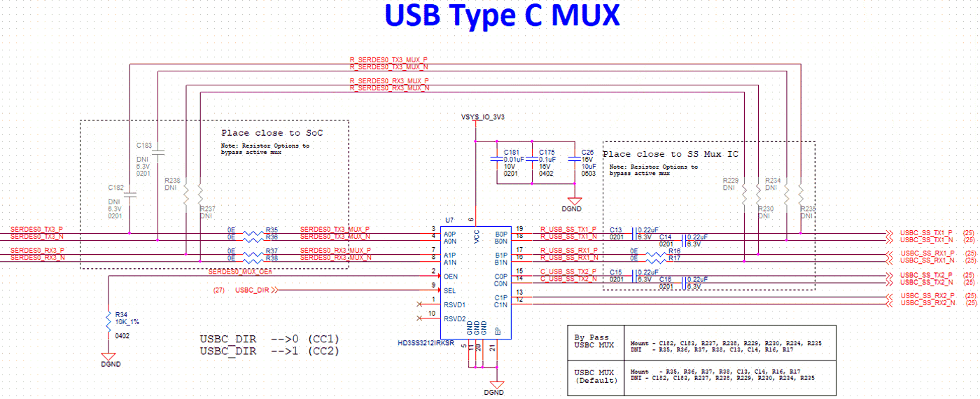
GUID-20200921-CA0I-XKPS-9GS8-SNZ1GVQSHGQH-low.png Figure 4-22 USB SS Mux Circuit

A CC and PD controller Mfr. Part# TUSB321RWBR and PTPS25830QWRHBTQ1 are used for CC detect, Port mapping and power delivery. This CC controller supports Dual Role Port (DRP), Downstream Facing Port (DFP) and Upstream Facing Port (UFP) modes, In CP board DRP, DFP and UFP modes can be selected through an EVM Configuration dip switch (SW3). The Dip switch settings are given in Table 6.
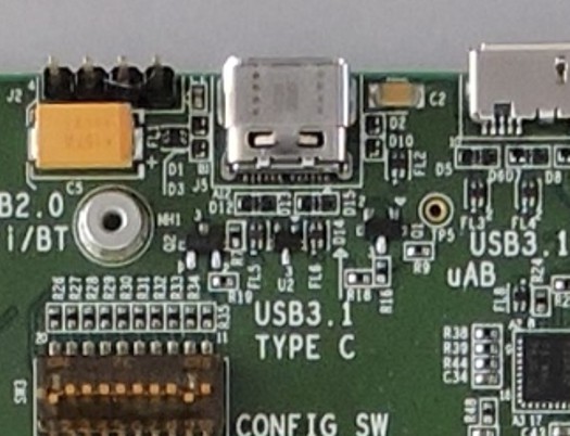
GUID-20200921-CA0I-WKVB-K8HT-XD2M1SZVGVT5-low.jpg Figure 4-23 USB3.1 Type C Interface

The AC coupling capacitors are provided on TX lines of Super speed signals, and common mode filters (MCZ1210DH900L2TA0G) are used at all the differential pairs. ESD protection diodes are provided on all required USB Signals (TPD1E05U06DPY for super speed signals and TPD2E2U06-Q1 for CC pins). TUSB321‘s Current Mode pin is pulled high through 499K resistor to set the Maximum Current Iout to 1.5A.
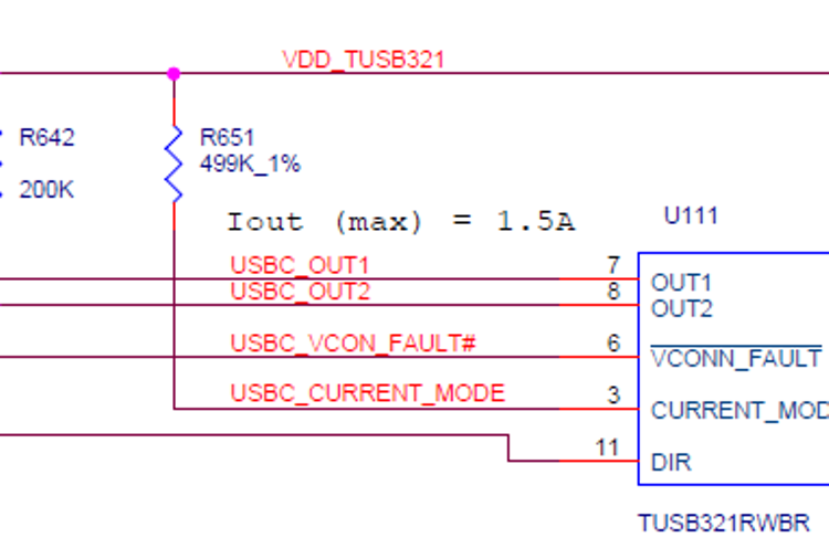
GUID-20200921-CA0I-V0WZ-3TT4-WPFPBMGFWSHV-low.png Figure 4-24 USB3.1 Type C Power Delivery Current Settings

The control signals for Powerdown and VBUS enable are given from I2C GPIO Expander2 (I2C add: 0x22 - P03) and the SoC DRVVBUS, respectively.