SWRU546E October   2018  – May 2022 AWR6843 , AWR6843AOP , IWR6443 , IWR6843 , IWR6843AOP


  1.   Trademarks
  2. 1Getting Started
    1. 1.1 Introduction
    2. 1.2 Key Features
      1. 1.2.1 Summary of Features
      2. 1.2.2 xWR6843ISK
      3. 1.2.3 IWR6843ISK-ODS (Overhead Detection Sensing)
      4. 1.2.4 IWR6843AOP
      5. 1.2.5 MMWAVEICBOOST
    3. 1.3 What’s Included
      1. 1.3.1 Kit Contents
        1. 1.3.1.1 xWR6843ISK
        2. 1.3.1.2 IWR6843ISK-ODS
        3. 1.3.1.3 IWR6843AOPEVM
        4. 1.3.1.4 MMWAVEICBOOST
  3. 2MMWAVEICBOOST
    1. 2.1 Hardware
    2. 2.2 Block Diagram and Features
      1. 2.2.1 Block Diagram
      2. 2.2.2 Hardware Features
    3. 2.3 Muxing Scheme for Multiple Sources
    4. 2.4 Using the MMWAVEICBOOST With the Starter Kit
      1. 2.4.1 PC Connection
      2. 2.4.2 Flashing the QSPI Flash on the Antenna Module
      3. 2.4.3 MMWAVEICBOOST and Antenna Module Connections for Modular Testing
    5. 2.5 Interfacing with the DCA1000EVM
      1. 2.5.1 mmWave Studio Interface
      2. 2.5.2 MMWAVEICBOOST and Antenna Module Configuration
      3. 2.5.3 DCA1000 EVM Connection
    6. 2.6 Power Connections
    7. 2.7 Connectors
      1. 2.7.1 20-Pin LaunchPad and Booster Pack Connectors (J5, J6)
      2. 2.7.2 60-Pin High Density (HD) Connector (J4 and J17)
      3. 2.7.3 60-Pin High Density (HD) Connector (J10)
      4. 2.7.4 MIPI 60-Pin Connector (J9)
      5. 2.7.5 TI 14-Pin JTAG Connector (J19)
      6. 2.7.6 CAN Connector (J1 and J2)
      7. 2.7.7 Ultra-Miniature Coaxial Connector (J3)
    8. 2.8 Jumpers, Switches and LEDs
      1. 2.8.1 Sense on Power (SOP) Jumpers
      2. 2.8.2 I2C Connections
        1. 2.8.2.1 Default I2C Address
        2. 2.8.2.2 43
        3. 2.8.2.3 3.3-V Rail Options
        4. 2.8.2.4 Miscellaneous Headers
        5. 2.8.2.5 Switches and LEDs
          1. 2.8.2.5.1 Switches
  4. 3xWR6843ISK / IWR6843ISK-ODS REV C
    1. 3.1  Hardware
      1. 3.1.1 xWR6843ISK EVM
      2. 3.1.2 IWR6843ISK-ODS EVM
    2. 3.2  xWR6843ISK/IWR6843ISK-ODS Block Diagram
    3. 3.3  PCB Storage and Handling Recommendations
    4. 3.4  Power Connections
      1. 3.4.1 Higher Power Applications
    5. 3.5  Interfaces
      1. 3.5.1 Switches, Buttons and Muxes
      2. 3.5.2 List of LEDs
      3. 3.5.3 CANFD
      4. 3.5.4 I2C Connections
        1. 3.5.4.1 EEPROM
        2. 3.5.4.2 Default I2C Address
    6. 3.6  xWR6843ISK Antenna
    7. 3.7  IWR6843ISK-ODS Antenna
    8. 3.8  Modular Mode
    9. 3.9  DCA1000EVM Mode
    10. 3.10 MMWAVEICBOOST Mode
  5. 4xWR6843AOPEVM Rev G
    1. 4.1  Hardware
    2. 4.2  Block Diagram
    3. 4.3  PCB Storage and Handling Recommendations
    4. 4.4  Heat Sink and Temperature
    5. 4.5  xWR6843AOPEVM Antenna
    6. 4.6  Switch Settings
    7. 4.7  xWR6843AOPEVM Muxing Scheme
      1. 4.7.1 SOP Configuration
    8. 4.8  Modular, DCA1000EVM and MMWAVEICBOOST Mode
      1. 4.8.1 Modular Mode
      2. 4.8.2 DCA1000EVM Mode
      3. 4.8.3 MMWAVEICBOOST Mode
    9. 4.9  Known Issues: Spurious Performance
    10. 4.10 PC Connection
      1. 4.10.1 Installing the Drivers
      2. 4.10.2 Flashing the Board
    11. 4.11 REACH Compliance
    12. 4.12 Regulatory Statements with Respect to the xWR6843AOPEVM Rev G
  6. 5xWR6843AOPEVM Rev F
    1. 5.1  Hardware
    2. 5.2  Block Diagram
    3. 5.3  PCB Storage and Handling Recommendations
    4. 5.4  Heat Sink and Temperature
    5. 5.5  xWR6843AOPEVM Antenna
    6. 5.6  Switch Settings
    7. 5.7  xWR6843AOPEVM Muxing Scheme
      1. 5.7.1 SOP Configuration
    8. 5.8  Modular and MMWAVEICBOOST Mode
      1. 5.8.1 Modular Mode
      2. 5.8.2 MMWAVEICBOOST Mode
    9. 5.9  PC Connection
      1. 5.9.1 Installing the Drivers
      2. 5.9.2 Flashing the Board
      3. 5.9.3 DCA1000
    10. 5.10 REACH Compliance
  7. 6IWR6843ISK / IWR6843ISK-ODS (deprecated)
    1. 6.1 Hardware
      1. 6.1.1 IWR6843ISK EVM
      2. 6.1.2 IWR6843ISK-ODS EVM
    2. 6.2 IWR6843ISK/IWR6843ISK-ODS Block Diagram
    3. 6.3 PCB Storage and Handling Recommendations
    4. 6.4 Power Connections
    5. 6.5 Miscellaneous and LEDs
      1. 6.5.1 List of LEDs
      2. 6.5.2 I2C Connections
        1. 6.5.2.1 EEPROM
        2. 6.5.2.2 Default I2C Address
    6. 6.6 IWR6843ISK Antenna
    7. 6.7 IWR6843ISK-ODS Antenna
  8. 7IWR6843AOPEVM (Deprecated)
    1. 7.1 Hardware
    2. 7.2 Block Diagram
    3. 7.3 PCB Storage and Handling Recommendations
    4. 7.4 IWR6843AOPEVM Antenna
    5. 7.5 Switch Settings
    6. 7.6 IWR6843AOPEVM Muxing Scheme
      1. 7.6.1 SOP Configuration
    7. 7.7 Modular and MMWAVEICBOOST Mode
      1. 7.7.1 Modular Mode
      2. 7.7.2 MMWAVEICBOOST Mode
    8. 7.8 PC Connection
      1. 7.8.1 Installing the Drivers
      2. 7.8.2 Flashing the Board
      3. 7.8.3 DCA1000
    9. 7.9 REACH Compliance
  9. 8TI E2E Community
  10. 9Certification Related Information
  11.   Revision History

Heat Sink and Temperature

Users are strongly encouraged to use the xWR6843AOPEVM with the heat sink installed. Due to the smaller size of the xWR6843AOPEVM, it is likely to get warmer than other larger sized EVMs on the mmWave Radar portfolioso care must be taken to ensure the junction temperature does not exceed 105°C. Figure 5-4 shows measurement of junction temperature versus duty cycle taken with and without the heat sink. As seen in the plot, the EVM can safely operate up to 50% duty cycle with or without the heat sink. Although the heatsink is not absolutely required, usage of the heat sink provides protection against exceeding the junction temperature at higher duty cyles.
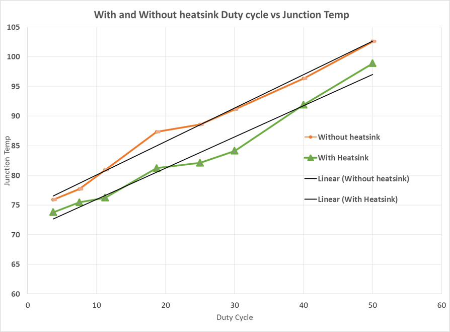
GUID-835E13AE-704B-4907-847C-241571844404-low.pngFigure 5-4 Duty Cycle versus Junction Temperature

When using the EVM for custom applications, the duty cycle can be adjusted as needed, the heat sink provided with the kit can be used, customers can also design their own heat sink using better heat disippating materials or one with more surface area such as addition of fins. The CAD drawing for the heat sink is shown in Figure 5-5
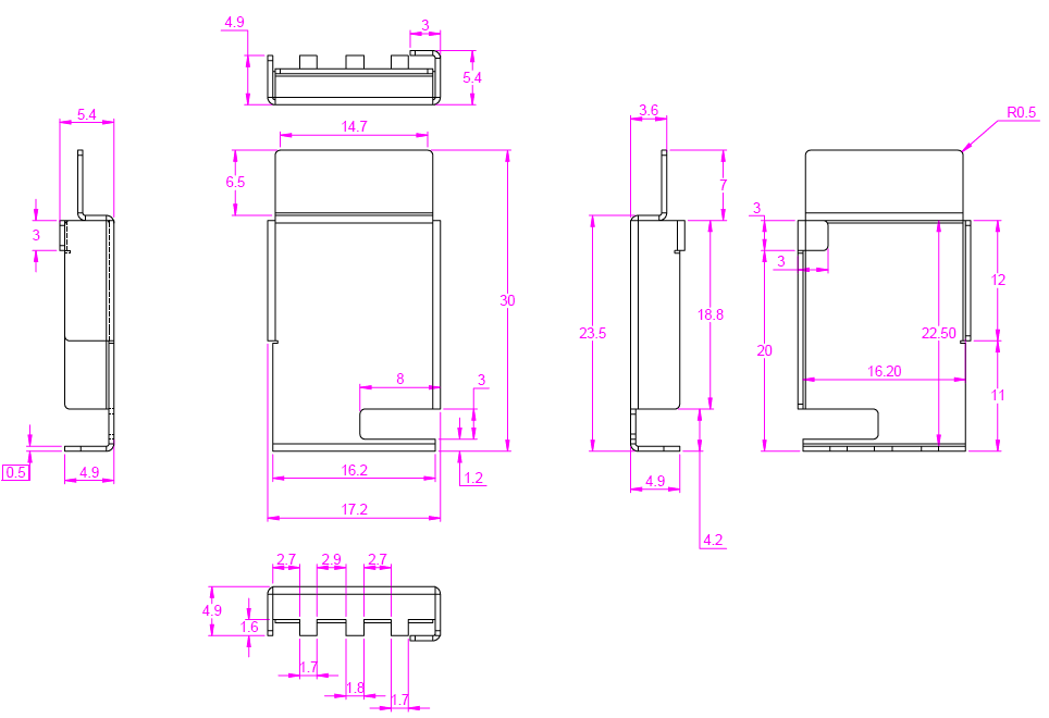
GUID-4E839D81-F171-40BA-A02A-30780743B445-low.pngFigure 5-5 Heat sink CAD drawing

Application of the heat sink is shown in Figure 5-6
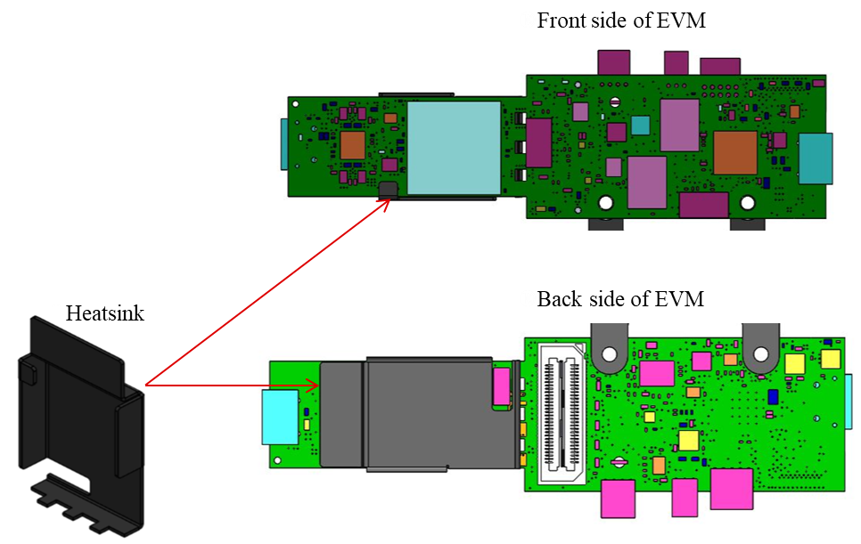
GUID-C6BE58BC-6287-4871-9582-F76DF29531F2-low.pngFigure 5-6 Heat sink placement