SWRU546E October 2018 – May 2022 AWR6843 , AWR6843AOP , IWR6443 , IWR6843 , IWR6843AOP
- Trademarks
- 1Getting Started
-
2MMWAVEICBOOST
- 2.1 Hardware
- 2.2 Block Diagram and Features
- 2.3 Muxing Scheme for Multiple Sources
- 2.4 Using the MMWAVEICBOOST With the Starter Kit
- 2.5 Interfacing with the DCA1000EVM
- 2.6 Power Connections
- 2.7
Connectors
- 2.7.1 20-Pin LaunchPad and Booster Pack Connectors (J5, J6)
- 2.7.2 60-Pin High Density (HD) Connector (J4 and J17)
- 2.7.3 60-Pin High Density (HD) Connector (J10)
- 2.7.4 MIPI 60-Pin Connector (J9)
- 2.7.5 TI 14-Pin JTAG Connector (J19)
- 2.7.6 CAN Connector (J1 and J2)
- 2.7.7 Ultra-Miniature Coaxial Connector (J3)
- 2.8 Jumpers, Switches and LEDs
- 3xWR6843ISK / IWR6843ISK-ODS REV C
-
4xWR6843AOPEVM Rev G
- 4.1 Hardware
- 4.2 Block Diagram
- 4.3 PCB Storage and Handling Recommendations
- 4.4 Heat Sink and Temperature
- 4.5 xWR6843AOPEVM Antenna
- 4.6 Switch Settings
- 4.7 xWR6843AOPEVM Muxing Scheme
- 4.8 Modular, DCA1000EVM and MMWAVEICBOOST Mode
- 4.9 Known Issues: Spurious Performance
- 4.10 PC Connection
- 4.11 REACH Compliance
- 4.12 Regulatory Statements with Respect to the xWR6843AOPEVM Rev G
- 5xWR6843AOPEVM Rev F
- 6IWR6843ISK / IWR6843ISK-ODS (deprecated)
- 7IWR6843AOPEVM (Deprecated)
- 8TI E2E Community
- 9Certification Related Information
- Revision History
2.8.2.5.1 Switches
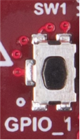
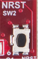
Table 2-14 shows the list of push buttons and usage.
Table 2-14 Switches Information
| Reference Designator | Usage | Comments | Image |
|---|---|---|---|
| SW1 | GPIO_1 | When pushed, the GPIO_1 is pulled to Vcc. |  Figure 2-26 SW1 Figure 2-26 SW1 |
| SW2 | RESET | This is used to RESET the mmWave Sensor device. This signal is also output on the 20-pin, 60-pin connectors and FTDI interfaces so an external processor can control the mmWave Sensor device. The onboard XDS110 can also control this reset. |  Figure 2-27 SW2 Figure 2-27 SW2 |
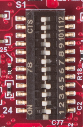
| S1.1 | CAN/SPI selection | OFF : SPI-1(default) ON : CAN |  Figure 2-28 S1 Switch Figure 2-28 S1 Switch |
| S1.2 | Header(J16) and 40 pin | OFF : J16 Header ON : 40 pin (default) | |
| S1.3 | Header(J16)/40 pin and FTDI | OFF : 40 pin/J16 header ON : FTDI (default) | |
| S1.4 | 60 pin and FTDI/40 pin/J16 | OFF : 60 pin ON : FTDI/J16 header/40 pin (default) | |
| S1.5 | 60 pin/FTDI/40 pin and XDS110 | OFF : 40/60 pin/FTDI ON : XDS110 (default) | |
| S1.6 | 60/40 pin and FTDI | OFF : 60/40 pin ON : FTDI (default) | |
| S1.7 | 60/40 pin and FTDI | OFF : 60/40 pin ON : FTDI (default) | |
| S1.8 | 40 pin and 60 pin | OFF : 60 pin (default) ON : 40 pin | |
| S1.9 | 40 pin and 60 pin | OFF : 60 pin (default) ON : 40 pin | |
| S1.10 | 40 pin and FTDI | OFF : 40 pin ON : FTDI (default) | |
| S1.11 | 40 pin and FTDI | OFF : 40 pin ON : FTDI (default) | |
| S1.12 | XDS110/14 pin | OFF : 14 pin ON : XDS110 (default) |
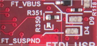
Table 2-15 provides the list of LEDs and usage.
Table 2-15 LEDs Information
| Reference Designator | Color | Usage | Comments | Image |
|---|---|---|---|---|
| DS1 | Yellow | nRESET | This LED is used to indicate the state of nRESET pin. If this LED is glowing, the device is out of reset. This LED will glow only after the 5-V supply is provided. |  Figure 2-29 DS1 Figure 2-29 DS1 |
| DS2 | Yellow | GPIO_2 | Glows when the GPIO_2 is logic 1 |  Figure 2-30 DS2 Figure 2-30 DS2 |
| DS3 | Red | NERROUT | Glows if there is any HW error in the xWR device |  Figure 2-31 LEDs Figure 2-31 LEDs |
| DS4 | Red | POWER | This LED indicates the presence of the 5-V supply. | |
| D5 | Yellow | SOR0 | SOR0 (SOP2) state | |
| D6 | Yellow | SOR1 | SOR1 (SOP1) state | |
| D7 | Yellow | SOR2 | SOR2 (SOP0) state | |
| D8 | Red | NRST | This LED is used to indicate the state of NRST pin. If this LED is glowing, the device is in reset state. | |
| D10 | Red | POWER | 3V3 supply indication | |
| D4 | Yellow | FTDI | Glows if the USB is in suspend mode |  Figure 2-32 D4 & D9 Figure 2-32 D4 & D9 |
| D9 | Red | POWER | 5-V supply indication (from USB bus) | |
| D11 | Green | POWER | 5-V supply indication if the input voltage to board is more than 5 V |  Figure 2-33 D11 & D14 Figure 2-33 D11 & D14 |
| D14 | Green | POWER | 3V3 supply indication |