SWRU546E October 2018 – May 2022 AWR6843 , AWR6843AOP , IWR6443 , IWR6843 , IWR6843AOP
- Trademarks
- 1Getting Started
-
2MMWAVEICBOOST
- 2.1 Hardware
- 2.2 Block Diagram and Features
- 2.3 Muxing Scheme for Multiple Sources
- 2.4 Using the MMWAVEICBOOST With the Starter Kit
- 2.5 Interfacing with the DCA1000EVM
- 2.6 Power Connections
- 2.7
Connectors
- 2.7.1 20-Pin LaunchPad and Booster Pack Connectors (J5, J6)
- 2.7.2 60-Pin High Density (HD) Connector (J4 and J17)
- 2.7.3 60-Pin High Density (HD) Connector (J10)
- 2.7.4 MIPI 60-Pin Connector (J9)
- 2.7.5 TI 14-Pin JTAG Connector (J19)
- 2.7.6 CAN Connector (J1 and J2)
- 2.7.7 Ultra-Miniature Coaxial Connector (J3)
- 2.8 Jumpers, Switches and LEDs
- 3xWR6843ISK / IWR6843ISK-ODS REV C
-
4xWR6843AOPEVM Rev G
- 4.1 Hardware
- 4.2 Block Diagram
- 4.3 PCB Storage and Handling Recommendations
- 4.4 Heat Sink and Temperature
- 4.5 xWR6843AOPEVM Antenna
- 4.6 Switch Settings
- 4.7 xWR6843AOPEVM Muxing Scheme
- 4.8 Modular, DCA1000EVM and MMWAVEICBOOST Mode
- 4.9 Known Issues: Spurious Performance
- 4.10 PC Connection
- 4.11 REACH Compliance
- 4.12 Regulatory Statements with Respect to the xWR6843AOPEVM Rev G
- 5xWR6843AOPEVM Rev F
- 6IWR6843ISK / IWR6843ISK-ODS (deprecated)
- 7IWR6843AOPEVM (Deprecated)
- 8TI E2E Community
- 9Certification Related Information
- Revision History
2.7.2 60-Pin High Density (HD) Connector (J4 and J17)
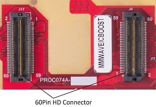
The 60-pin HD connector shown in Figure 2-18 provides the high-speed CSI/LVDS data, controls signals (SPI, UART, I2C, NRST, NERR, and SOPs) and JTAG debug signals from the starter kit. The Trace and DMM interface lines are also available through this connector.
 Figure 2-18 60-Pin HD Connectors
Table 2-6 and Table 2-7 list the 60-pin HD connector pinout.
Table 2-6 J4 Connector Pinout
| Pin Number | Pin Description | Pin Number | Pin Description |
|---|---|---|---|
| 1 | 1V | 31 | DP2 |
| 2 | 5V | 32 | GND |
| 3 | 1V | 33 | DP3 |
| 4 | 3.3V | 34 | LVDS_CLKP |
| 5 | 1.2V | 35 | DP4 |
| 6 | 3.3V | 36 | LVDS_CLKM |
| 7 | 1.2V | 37 | DP5 |
| 8 | DMM_SYNC | 38 | GND |
| 9 | 1.8V | 39 | DP6 |
| 10 | DMM_CLK | 40 | LVDS_1P |
| 11 | JTAG_TDI | 41 | DP7 |
| 12 | NRST | 42 | LVDS_1M |
| 13 | JTAG_TMS | 43 | BSS_LOGGER |
| 14 | PGOOD | 44 | GND |
| 15 | JTAG_TCK | 45 | OSC_CLKOUT |
| 16 | HOST_INTR1 | 46 | LVDS_0P |
| 17 | JTAG_TDO/SOP0 | 47 | MCU_CLKOUT |
| 18 | MSS_LOGGER | 48 | LVDS_0M |
| 19 | SPI_CS1 | 49 | PMIC_CLKOUT/SOP2 |
| 20 | GND | 50 | GND |
| 21 | SPI_CLK1 | 51 | WARMRST |
| 22 | SYNC_IN | 52 | NERRIN |
| 23 | SPI_MOSI1 | 53 | SDA |
| 24 | SYNC_OUT/SOP1 | 54 | NERROUT |
| 25 | SPI_MISO1 | 55 | SCL |
| 26 | GND | 56 | GPIO_0 |
| 27 | DP0 | 57 | RS232_RX |
| 28 | LVDS_FRCLKP | 58 | GPIO_1 |
| 29 | DP1 | 59 | RS232_TX |
| 30 | LVDS_FRCLKM | 60 | GPIO_2 |
Table 2-7 J17 Connector Pinout
| Pin Number | Pin Description | Pin Number | Pin Description |
|---|---|---|---|
| 1 | 5V | 31 | GND |
| 2 | 5V | 32 | LVDS_3P |
| 3 | 5V | 33 | GND |
| 4 | VPP_1.7V | 34 | LVDS_3M |
| 5 | GND | 35 | NC |
| 6 | NC | 36 | GND |
| 7 | 3.3V | 37 | NC |
| 8 | NC | 38 | LVDS_2P |
| 9 | 3.3V | 39 | NC |
| 10 | NC | 40 | LVDS_2M |
| 11 | PMIC_EN | 41 | NC |
| 12 | NC | 42 | GND |
| 13 | DP8 | 43 | NC |
| 14 | NC | 44 | NC |
| 15 | DP9 | 45 | NC |
| 16 | NC | 46 | NC |
| 17 | DP10 | 47 | NC |
| 18 | GND | 48 | NC |
| 19 | DP11 | 49 | NC |
| 20 | LVDS_VALIDP | 50 | NC |
| 21 | DP12 | 51 | NC |
| 22 | LVDS_VALIDM | 52 | NC |
| 23 | DP13 | 53 | NC |
| 24 | GND | 54 | NC |
| 25 | DP14 | 55 | NC |
| 26 | NC | 56 | NC |
| 27 | DP15 | 57 | NC |
| 28 | NC | 58 | NC |
| 29 | GND | 59 | NC |
| 30 | GND | 60 | NC |