TIDUDT4A May   2018  – November 2021 AM3351 , AM3352 , AM3354 , AM3356 , AM3357 , AM3358 , AM3358-EP , AM3359


  1.   Description
  2.   Resources
  3.   Features
  4.   Applications
  5.   5
  6. 1System Description
    1. 1.1 Key System Specifications
  7. 2System Overview
    1. 2.1 Block Diagram
    2. 2.2 Design Considerations
      1. 2.2.1 Power Rails Requirements of the System
      2. 2.2.2 Power Sequencing Requirements of the System
      3. 2.2.3 Uncontrolled Power Off
      4. 2.2.4 12-V Input Voltage Rail
    3. 2.3 Highlighted Products
      1. 2.3.1 TLV62568/9
      2. 2.3.2 LM3881
      3. 2.3.3 TLV803
      4. 2.3.4 AM335x
      5. 2.3.5 WL1837MOD
    4. 2.4 System Design Theory
      1. 2.4.1 Power Tree Architecture
      2. 2.4.2 Power Sequencing Solution
        1. 2.4.2.1 Design Steps for DC-DCs
        2. 2.4.2.2 Design Steps for the Sequencer
        3. 2.4.2.3 Design Steps for the Supervisor
  8. 3Hardware, Software, Testing Requirements, and Test Results
    1. 3.1 Required Hardware and Software
      1. 3.1.1 Hardware
        1. 3.1.1.1 Connector Configuration of TIDA-01568
        2. 3.1.1.2 Procedure for Board Bring-up and Testing
      2. 3.1.2 Software
        1. 3.1.2.1 Description of Environment Implementation
        2. 3.1.2.2 How to Customize the Processor SDK for This Reference Design
      3. 3.1.3 Software Bring-up Tips
    2. 3.2 Testing and Results
      1. 3.2.1 Test Setup
      2. 3.2.2 Test Results
        1. 3.2.2.1 Power-Up and Power-Down Sequence Test
        2. 3.2.2.2 Typical Characteristics of DC-DCs
  9. 4Design Files
    1. 4.1 Schematics
    2. 4.2 Bill of Materials
    3. 4.3 PCB Layout Recommendations
      1. 4.3.1 PCB Layout Guidelines
      2. 4.3.2 Layout Prints
    4. 4.4 Altium Project
    5. 4.5 Gerber Files
    6. 4.6 Assembly Drawings
  10. 5Software Files
  11. 6Related Documentation
    1. 6.1 Trademarks
  12. 7About the Author
  13. 8Revision History

Design Steps for the Sequencer

Select the suitable sequencer offering 3 power up and power down sequencing orders in regard to the power tree architecture. Cost, space, and ease-of-use are the key concerns for the sequencer.

In this design, the LM3881 provides a simple solution for sequencing multiple rails in a controlled manner. A small external timing capacitor (C2) establishes the clock waveform; the relationship between the capacitor and the clock period is typically 120 µs/nF. In this design, a 10-nF capacitor is used, which means the clock period is 1.2 ms. The delay time between the 3 flags is 8 clock cycles, which means the interval time between power rails is 9.6 ms.

A resistor divider can also be used to enable the LM3881, based on exceeding a certain VCC supply voltage threshold. The supply voltage for which EN is asserted is given in Equation 6.

Equation 6. GUID-D3AD7A10-FE94-4FCC-A67F-B461E0DF46B2-low.gif

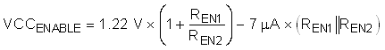
By tuning the capacitor, the delay time can be adjusted for a different discharge time. By tuning the VCC supply voltage threshold, the moment when the sequencer works also can be adjusted for a different discharge time.