TIDUDT4A May 2018 – November 2021 AM3351 , AM3352 , AM3354 , AM3356 , AM3357 , AM3358 , AM3358-EP , AM3359
- Description
- Resources
- Features
- Applications
- 5
- 1System Description
- 2System Overview
- 3Hardware, Software, Testing Requirements, and Test Results
- 4Design Files
- 5Software Files
- 6Related Documentation
- 7About the Author
- 8Revision History
2.3.1 TLV62568/9
This reference design selected the TLV62568 with a 1-A output current and the TLV62569P with a 2-A output current.
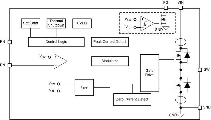
The TLV62568/9 is a high-efficiency synchronous step-down converter. The device operates with an adaptive off time with a peak current control scheme. The device typically operates at a 1.5-MHz frequency pulse width modulation (PWM), at moderate to heavy load currents. Based on the VIN/VOUT ratio, a simple circuit sets the required off time for the low-side MOSFET, making the switching frequency relatively constant regardless of the variation of input voltage, output voltage, and load current.
Figure 2-4 shows the functional block diagram of the TLV62568, and as a reference diagram for the TLV62569.
 Figure 2-4 TLV62568 Functional Block Diagram
Features:
- Up to 95% Efficiency
- Low R DS(ON) Switches 150 mΩ / 100 mΩ
- 2.5-V to 5.5-V Input Voltage Range
- Adjustable Output Voltage from 0.6 V to VIN
- Power Save Mode for Light Load Efficiency
- 100% Duty Cycle for Lowest Dropout
- 35-µA Operating Quiescent Current
- 1.5-MHz Switching Frequency
- Power Good Output
- Over Current Protection
- Internal Soft Startup
- Thermal Shutdown Protection
- Available in SOT Package
- Pin-to-Pin Compatible with TLV62569