TIDUEB8C July 2018 – March 2021 TPS274160
- Description
- Resources
- Features
- Applications
- 5
- 1System Description
- 2System Overview
- 3Hardware, Software, Testing Requirements, and Test Results
- 4Design Files
- 5Software Files
- 6Related Documentation
- 7About the Author
- 8Revision History
2.2.1 LM5165
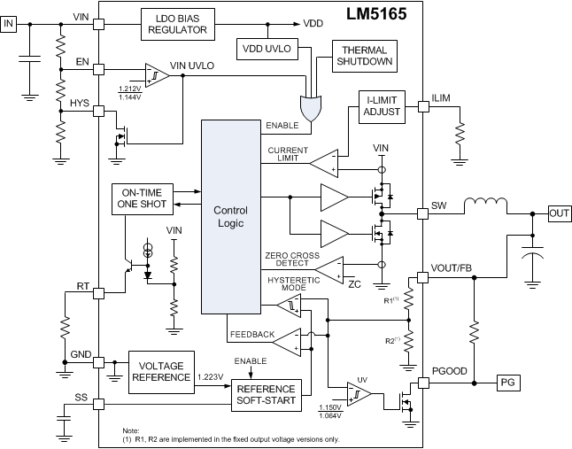
The LM5165 converter is an easy-to-use synchronous buck DC-DC regulator that operates from a 3-V to 65-V supply voltage. The device is intended for step-down conversions from 3.3-V, 5-V, 12-V, 24-V, and 48-V unregulated, semi-regulated and fully-regulated supply rails. With integrated high-side and low-side power MOSFETs, the LM5165 delivers up to 150-mA DC load current with high efficiency and ultra-low input quiescent current in a very small solution size. Designed for simple implementation, a choice of operating modes offers flexibility to optimize its usage according to the target application. In constant on-time (COT) mode of operation, ideal for low-noise, high current, fast load transient requirements, the device operates with predictive on-time switching pulse. A quasi-fixed switching frequency over the input voltage range is achieved by using an input voltage feedforward to set the on-time. Alternatively, pulse frequency modulation (PFM) mode, complemented by an adjustable peak current limit, achieves exceptional light-load efficiency performance. Control-loop compensation is not required with either operating mode, reducing design time and external component count.
 Figure 2-2 LM5165 Block Diagram
Key features relevant for this design are:
- Wide input voltage range of 3 V to 65 V
- Fixed 3.3-V output voltages
- 150-mA synchronous buck converter
- Integrated 2-Ω PMOS buck switch
- Integrated 1-Ω NMOS synchronous rectifier
- Eliminates external rectifier diode
- Selectable PFM or COT mode operation
- No loop compensation or bootstrap components