TIDUEB8C July   2018  – March 2021 TPS274160


  1.   Description
  2.   Resources
  3.   Features
  4.   Applications
  5.   5
  6. 1System Description
    1. 1.1 Key System Specifications
  7. 2System Overview
    1. 2.1 Block Diagram
    2. 2.2 Highlighted Products
      1. 2.2.1 LM5165
      2. 2.2.2 TLC59282
      3. 2.2.3 TPS4H160-Q1
      4. 2.2.4 INA253
      5. 2.2.5 TIOL111
    3. 2.3 System Design Theory
      1. 2.3.1 IO-Link PHY
      2. 2.3.2 Current Sink
      3. 2.3.3 Power Supply for L+
      4. 2.3.4 Power Supply
      5. 2.3.5 Pinouts
    4. 2.4 Software Frame Handler
      1. 2.4.1 PRU-ICSS IO-Link Frame-Handler
        1. 2.4.1.1 Performance Advantages and Benefits
        2. 2.4.1.2 Principle of Operation
  8. 3Hardware, Software, Testing Requirements, and Test Results
    1. 3.1 Required Hardware and Software
      1. 3.1.1 Hardware
      2. 3.1.2 Software
    2. 3.2 Testing and Results
      1. 3.2.1 Test Setup
      2. 3.2.2 Test Results
        1. 3.2.2.1 IO-Link Wake-Up Pulse
        2. 3.2.2.2 L+ Turnon Behavior
        3. 3.2.2.3 Current Sink on CQ
        4. 3.2.2.4 Residue Voltage
        5. 3.2.2.5 IO-Link Physical Layer Test Summary
        6. 3.2.2.6 Current Sense on Each Port
        7. 3.2.2.7 TPS4H160 Thermal Behavior
  9. 4Design Files
    1. 4.1 Schematics
    2. 4.2 Bill of Materials
    3. 4.3 PCB Layout Recommendations
      1. 4.3.1 Layout Prints
    4. 4.4 Altium Project
    5. 4.5 Gerber Files
    6. 4.6 Assembly Drawings
  10. 5Software Files
  11. 6Related Documentation
    1. 6.1 Trademarks
  12. 7About the Author
  13. 8Revision History

Current Sink

Beside the wake-up pulse, the master PHY has a second important difference to the device PHY shown in Figure 2-8. It has to include a current sink. Since the TIOL111 device does not include this in the chip, it is implemented on the board.
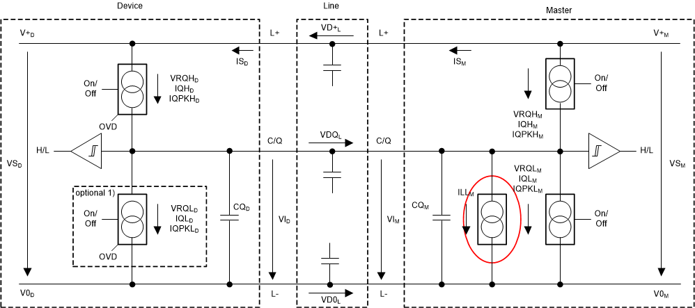
GUID-75AF1F01-79D6-4B42-BE98-3D2E345E448F-low.gif Figure 2-8 Block Diagram IO-Link® System

As the excerpt of the specification in Table 2-3 shows, the current has to be between 5 mA to 15 mA.

Table 2-3 Specification for IO-Link® Master Current Sink(1)
ILLM Load or discharge current for:
0 V < VIM < 5 V
5 V < VIM < 15 V
15 V < VIM < 30 V


5
 
N/A
N/A 
N/A
 
15 
15 
15
 
mA
mA
mA
Currents are compatible with the definition of type 1 digital inputs in IEC 61131-2. However, for the range 5 V < VIM < 15 V, the minimum current is 5 mA instead of 2 mA in order to achieve short enough slew rates for pure p-switching devices.

Implementing such a small and tolerable current sink that is only active when the transmitter is disabled can be done with a simple NPN transistor.

GUID-0CBB7E8E-B56F-42F4-BE02-F7B6172C88A7-low.svg Figure 2-9 Simple Current Sink

Figure 2-9 shows the schematic. The current sink is controlled by the TX line coming from the MCU and going to the TIOL111 device. Since the logic of the TIOL111 device is inverting and the default level on the TX line is high in idle state, this will enable the current sink whenever the driver is disabled or transmitting a 0 V on the CQ line. So it does not increase the current consumption in normal operation.